@gsuberland Yeah I might have to add that lol.
Let me finish collecting data from the other rails then we'll see
Security and open source at the hardware/software interface. Embedded sec @ IOActive. Lead dev of ngscopeclient/libscopehal. GHz probe designer. Open source networking hardware. "So others may live"
Toots searchable on tootfinder.
@gsuberland Yeah I might have to add that lol.
Let me finish collecting data from the other rails then we'll see
@johnlogic First step for me is to take a measurement closer to the IC and see if this is even an issue.
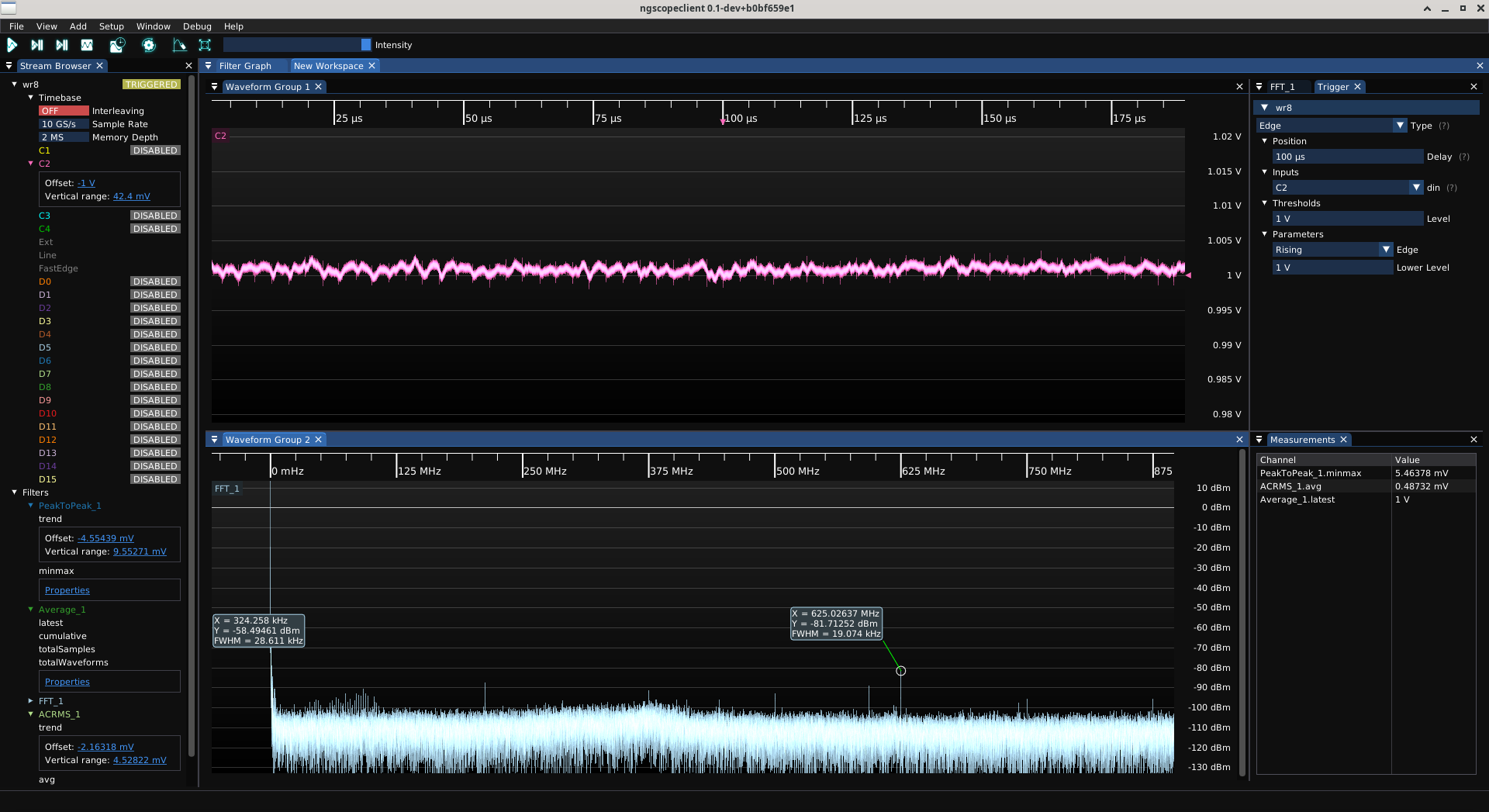
My other rail test points are on the far side of the BGA package footprint and are reading far lower, e.g. 1V0_2 is 5.4 mV p-p and 487 μV RMS.
So this might just be that I'm reading switching noise as a result of being too close to the DC-DC before any of the high freq caps have had a chance to do their job.
@johnlogic On a single cycle or integrated abs(delta) over the entire ringing period?
@gsuberland Yep that's my thought.
Here's what 1V0_2 at the left side test point looks like
@gsuberland So I'm wondering if maybe my test point is just at a noisy location along the plane and measuring under the PHY would give better results.
I'm gonna solder the RP4030 coax probe across some caps closer to the PHY in a bit, but want to finish grabbing all the data I can from the top side without decabling first
@gsuberland Here's layout of L1 outer signal + L3 power plane with the 1V0 zone fill highlighted. Test point is just east of the PSU area
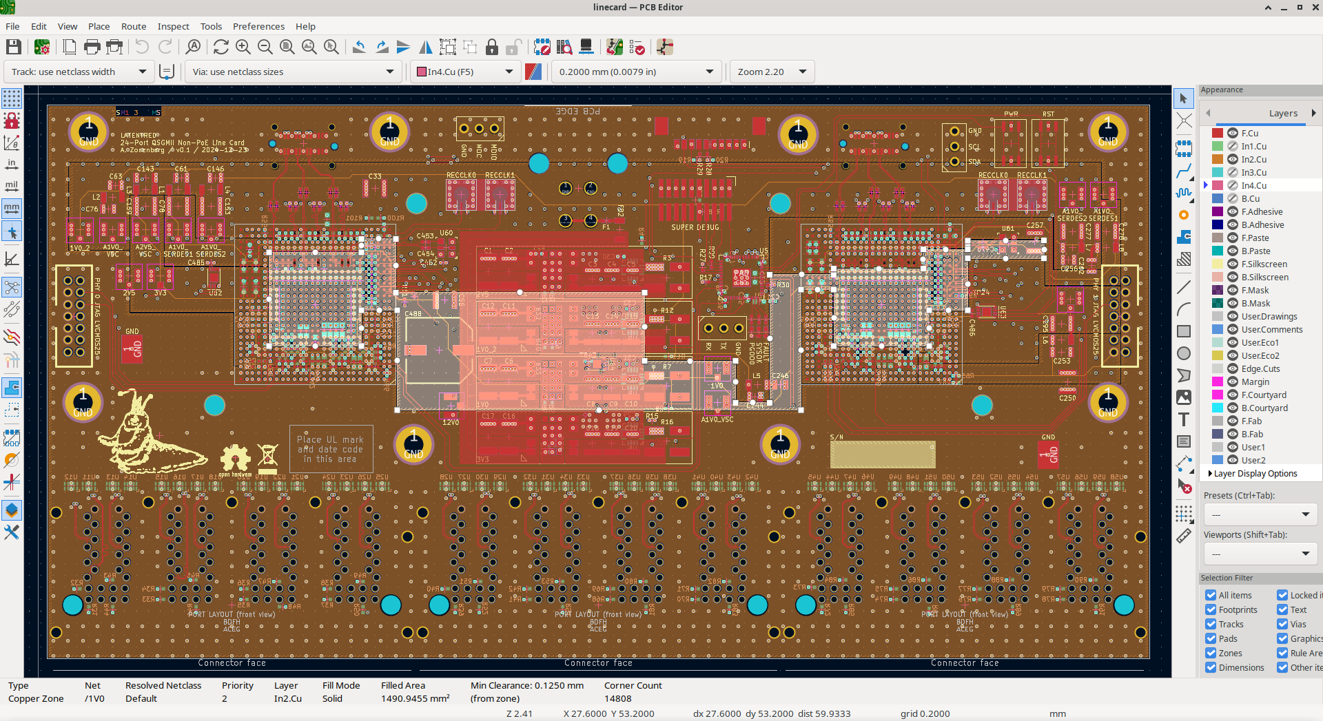
@gsuberland So this board has two separate 1.0V power domains, 1V0 and 1V0_2.
Both use identical DC-DC converter layouts.
1V0 drives the digital core of both PHYs directly with no filtering.
1V0_2 drives three separate analog rails for each PHY (one for PLL/PHY stuff, plus two separate domains for the SERDES), for a total of six, through separate ferrite bead + cap pi filters.
1V0_2 has vastly lower noise (487 μV RMS / 5.6 mV p-p) at my test point.
Possibly relevant is that the 2V5 and 1V0_2 test points are at the far left side of the board (after passing one of the PHYs and all its local caps) while the 1V0 test point is right next to the DC-DC.
@johnlogic And yes there very likely is some data leakage there although you'd be looking at the combination of all 24 ports on the board.
But that's not a side channel I am particularly concerned about.
@johnlogic I'm not worried about the sawtooth, it's like 5 mV lol. Even my most sensitive rails have like 10 mV ripple tolerance.
It's the 40 mV spikes that I'm concerned about.
@gsuberland Stackup is 6L:
* L1: Components, some zone fills in PSU area, a few low speed control signals
* L2: Solid ground
* L3: Power pours
* L4: Power pours plus the low-speed signal traces for the port indicator LEDs
* L5: Solid ground
* L6: All of the Ethernet diff pairs, some low speed signals
The 5 Gbps QSGMII traces are on L1/L6 and very short (~1cm) to the ARF6 connectors.
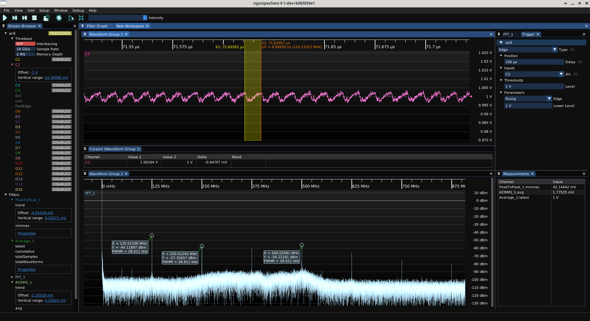
@gsuberland The "500 MHz" is a very rough estimate based on cursors, I don't think it's literally coming from the PHY.
It's not a strong 500 MHz spectral line that's always present, it's the 300 kHz switching transients have a few cycles of ~500 MHz before damping out. Which is why I'm suspecting the PDN rather than the PHY.
@gsuberland I feel like the combo 220 vs 330 is not a great idea, but they're both so large that I would not expect any resonances between them to show up as 500 MHz ringing on switching transients. Any problems they cause I'd expect to show up much lower down.
@gsuberland thoughts?
There's two 220 uF 1210 MLCCs directly on the converter output, plus a third footprint which is currently unpopulated (reserved in case I needed additional low frequency capacitance).
Additionally, each PHY has a 330 uF 1210 bulk cap next to it (this might be a mistake vs the 220, possibly causing resonances?), six 4.7 uF 0603s for mid band, and 40 0.47 uF 0402s (one per power/ground ball pair) for high band.
The big difference is that the measurement point for 1V0 that I took these readings from is right next to the regulator, whereas the 2V5 test point is at the far side of a PHY and probably has some attenuation due to the PHY PDN (inductance of the power plane plus local bypass caps forming an L-C LPF)
Maybe I should repeat my 1V0 measurement under the PHY and see how different it looks there?
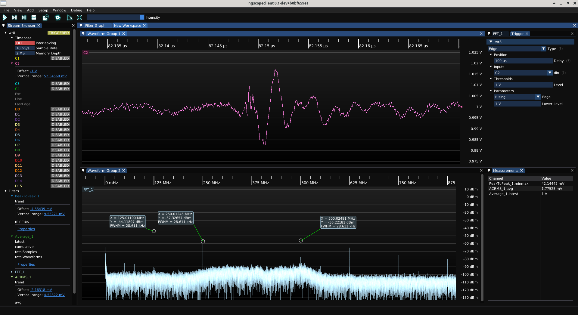
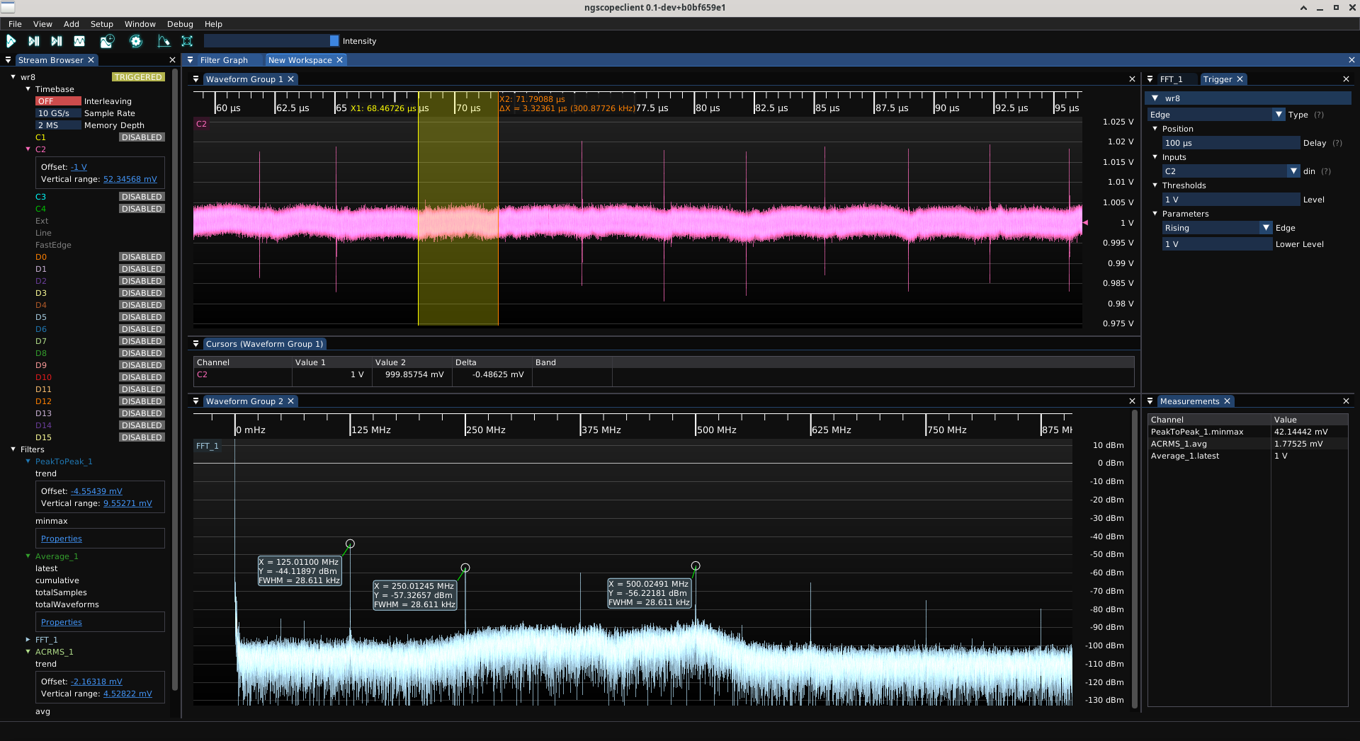
So this power rail is interesting. It's 1.775 mV RMS and 42 mV p-p.
~5 mV p-p of 125 MHz triangular ripple (core operating frequency of the two Ethernet PHYs on the board, plus also ~500 MHz ringing on the 300 kHz switching transients reaching 42 mV p-p (+/- 21 mV).
This is probably not enough to cause any problems, all of the 1.0V supplies on the PHY are specced at +/- 50 mV, but I don't like ripple :P
Like 2V5, this rail is generated by a MYMGK00504ERSR, but the switching spikes are massively stronger which is interesting given how similar the PDNs for each rail are at first glance.
@jpm this is a tub and curtain setup. I've actually come out pretty dry most times
Little one has reached an interesting stage of personal hygiene. She wants to shower instead of taking baths, but can't do it fully by herself.
So i have to poke my head and arms around the shower curtain, soap up her head, rinse her hair without getting water in her eyes, and try not to get myself completely drenched in the process or fling too much water around the bathroom.
@axel_hartmann @whoami Huh, I was under the impression that containers were normally sorted by type as solids and only *then* separated and shredded as relatively homogeneous materials.
Back when I was a kid we had separate recycling cans for HDPE/LDPE, metal, clear glass, green glass, and brown glass.
@dotstdy Yeah I know, that's why I was confused. Like, it seemed silly to go through all this engineering effort to hold onto a tiny bit of what's essentially garbage and isn't going to be usefully recycleable anyway.