The Unreasonable Machine: How ASML’s EUV Lithography Saved Moore’s Law
How ASML’s EUV Lithography | Chip Manufacturing
The Most Important Machine in the World: ASML EUV Lithography
In the silent, vibration-controlled clean rooms of the world’s most advanced semiconductor factories, machines worth over $400 million perform a miracle of precision 24 hours a day. They are the reason the smartphone in your pocket possesses more computing power than the guidance systems that took Apollo astronauts to the moon. These machines, known as Extreme Ultraviolet (EUV) lithography systems, are the pinnacle of human engineering and the unsung guardians of technological progress. For over three decades, their development was deemed nearly impossible, a fool’s errand that defied the laws of physics and tested the limits of material science. Yet, today, a single company from the Netherlands, ASML, builds them, making it perhaps the most strategically important technology firm on the planet. This is the story of unreasonable ambition, of scientists laughed off stages, and of the machine that refused to let Moore’s Law die.
The Brick Wall: Moore’s Law Grinds to a Halt
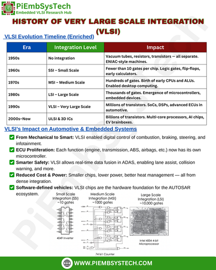
The journey begins with a fundamental truth of the digital age: smaller transistors mean faster, more powerful, and more efficient computers. For fifty years, the industry followed “Moore’s Law,” the observation by Intel co-founder Gordon Moore that the number of transistors on a chip doubled roughly every two years. This relentless miniaturization was driven by advances in photolithography—the process of “printing” circuit patterns onto silicon wafers using light. Engineers simply used shorter wavelengths of light to draw ever-finer lines.
By the late 1990s, the industry had settled on using 193-nanometer deep ultraviolet light. But as the 2010s approached, a brick wall loomed. The features chipmakers needed to print were becoming smaller than the wavelength of the light itself, leading to blurry, unusable patterns. The industry employed ingenious multpatterning techniques, etching patterns multiple times to squeeze out smaller features, but this was a costly and complex workaround. By around 2015, progress was stalling. The economic engine of the tech world, Moore’s Law, was in genuine peril. The industry desperately needed a leap to a radically new wavelength, one so short it existed only in theory and in the heart of the sun: Extreme Ultraviolet light at 13.5 nanometers.
The Impossible Problem: Building a Sun on Earth
The idea of using EUV light for lithography was first proposed in the 1980s by Japanese physicist Hiroo Kinoshita. It was immediately seen as preposterous. EUV light behaves less like visible light and more like an X-ray. It is absorbed by almost everything—air, lenses, and even the mirrors in a standard microscope. To use it, the entire process would have to occur in a vacuum. More critically, you couldn’t use traditional lenses to focus the light, as they would absorb it instantly. Kinoshita’s early presentations were met with extreme skepticism; his peers considered it “a big fish story.”
The core challenges were threefold and each seemed insurmountable. First, you needed to create the light. There is no natural EUV source on Earth. The solution was to create microscopic, man-made stars—superheating tiny tin droplets to a plasma state over 220,000 Kelvin, roughly 40 times hotter than the surface of the sun. This had to be done not once, but 50,000 times per second, with unerring accuracy.
Second, you needed to collect and focus the light. Since lenses were impossible, the only hope was to use mirrors. But standard mirrors absorb EUV light. The breakthrough came from adapting multilayer mirrors, developed for X-ray telescopes, which could reflect a small percentage of EUV light by using carefully layered stacks of atoms. To make a functional optical system, however, these mirrors needed to be the smoothest objects ever created by humankind. If scaled to the size of Germany, the largest imperfection on their surface would be just one millimeter high.
Third, you needed near-perfect alignment. A modern chip has over 100 layers that must be stacked with atomic precision. The overlay accuracy—the tolerance for misalignment between layers—is less than 1.5 nanometers. To achieve this while the machine’s internal components whip around at over 20 Gs of acceleration is a feat of control engineering that borders on magic.
The Unreasonable Pioneers: From Mockery to Milestone
For years, EUV was a project pursued only in national labs, like Lawrence Livermore in the US, where scientists like Andy Hawryluk worked on multilayer mirrors for imaging nuclear fusion reactions. When Hawryluk first proposed applying the technology to chipmaking at a conference, he was “literally laughed off the stage.” It was a career low point. Yet, a seed had been planted. Key industry players, realizing the 193-nanometer dead end was approaching, began to take notice. A consortium was formed, but the engineering challenges were so vast and expensive that, one by one, American tech giants like Intel and Motorola backed away from building the complete machine.
This left the field to an unlikely champion: ASML, a relatively small company from Veldhoven, Netherlands, that had spun out of Philips. Led by visionaries like Martin van den Brink and Jos Benschop, ASML made an “unreasonable” bet. They committed to solving the entire EUV puzzle, partnering with German optics master Zeiss for the mirrors. The journey was a marathon of failure and iteration. Early plasma sources generated only 11 watts of power—nowhere near the 250+ watts needed for commercial production. Tin debris from the plasma explosions constantly coated and ruined the priceless mirrors.
The breakthrough came from a shift in strategy. Instead of hitting a single tin droplet with one laser pulse, engineers devised a “pre-pulse” technique. A first laser pulse shapes the droplet into a pancake; a second, more powerful pulse then vaporizes it into a low-density plasma, dramatically increasing EUV output while reducing debris. It was a masterstroke of precision, akin to hitting a speeding bullet with a second bullet to make it explode more efficiently—50,000 times per second.
The Crown Jewel: Inside the EUV Machine
Today’s EUV machine is a cathedral of technology. It is assembled in a clean room 10,000 times cleaner than a hospital operating room. The machine itself is a network of modules: the powerful CO2 laser system, the complex vacuum chamber where tin droplets turn into plasma, the illuminator with its atomically smooth mirrors, and the precision stage that moves the silicon wafer with nanometer accuracy.
The scale is breathtakingly inverse to its purpose. To draw features just a few atoms wide, the machine is the size of a bus, weighs over 200 tons, and requires 250 crates transported in 20 trucks and three cargo planes to ship. It contains over 100,000 parts sourced from 5,000 suppliers worldwide. It is, as the video narrator states, “the most complicated commercial product humanity has ever built.”
ASML’s monopoly on this technology makes it the linchpin of the global tech economy. Its high-NA (Numerical Aperture) EUV machines, the next generation, are already pushing the boundaries further, ensuring Moore’s Law continues for years to come. Every advanced processor from TSMC, Samsung, and Intel—the brains behind everything from data centers to AI models—is made with an ASML machine.
The Triumph of Unreasonable Persistence
The story of EUV lithography is a testament to human ingenuity and stubborn perseverance in the face of unanimous doubt. It took over 30 years, tens of billions of dollars in investment, and the concerted effort of thousands of scientists and engineers to turn an “impossible” physics problem into the backbone of modern civilization. It proves that the greatest technological leaps are often achieved not by those who adapt to the world’s limits, but by the “unreasonable” ones who strive to change the world’s limits themselves. As we hold a device containing billions of perfectly formed transistors, we hold the result of that unreasonableness—a miracle, manufactured.
👉 Share your thoughts in the comments, and explore more insights on our Journal and Magazine. Please consider becoming a subscriber, thank you: https://borealtimes.org/subscriptions – Follow The Boreal Times on social media. Join the Oslo Meet by connecting experiences and uniting solutions: https://oslomeet.org
References & Further Reading
- Hijink, Marc. “Focus: The ASML Way.” (Book detailing ASML’s history and EUV development).
- Stewart, Jayson. “The Supernova in the Machine.” IEEE Spectrum, 2024. https://spectrum.ieee.org/euv-light-source-supernova


