#ASICDesign

MosChip®MosChipTech
2025-11-10

Your full-lifecycle Turnkey ASIC partner - from RTL to Volume Production.

MosChip brings in multi-node expertise (180 to 2nm) and a proven record of successful tape-outs, delivering with first-time right silicon.

Let's connect for your silicon journey!

zurl.co/MArLK

2025-09-22

So here are the photos of the actual chip, taken with a microscope. The black rectangle censors my name. I placed a steel ruler next to the chip in one of the photos to give you an idea of how small it really is. Each black line corresponds to 1 mm

The artwork on the chip is from OggyTheFox (@oggythefox.bsky.social on Bluesky)

In the second picture, you can see that there's always a second chip next to my chip. I don't know what kind of chip it is or why it wasn't separated from mine, but it at least makes the whole thing a little easier to handle because it makes it physically larger x3

I have five chips without a package and five have been bonded into a package, so I'm currently designing a PCB so I can test if the chip works :3

#electronics #asic #asicdesign

Photo of the chip next to a steel ruler, together with the other chip it is 5 mm long.On the right side is my chip (the slightly shorter one). On the left side, you can see another chip that isn't from me.Close-up shot of my chip, showing the artwork on the right side. The silver squares are the bond pads.
2025-09-21

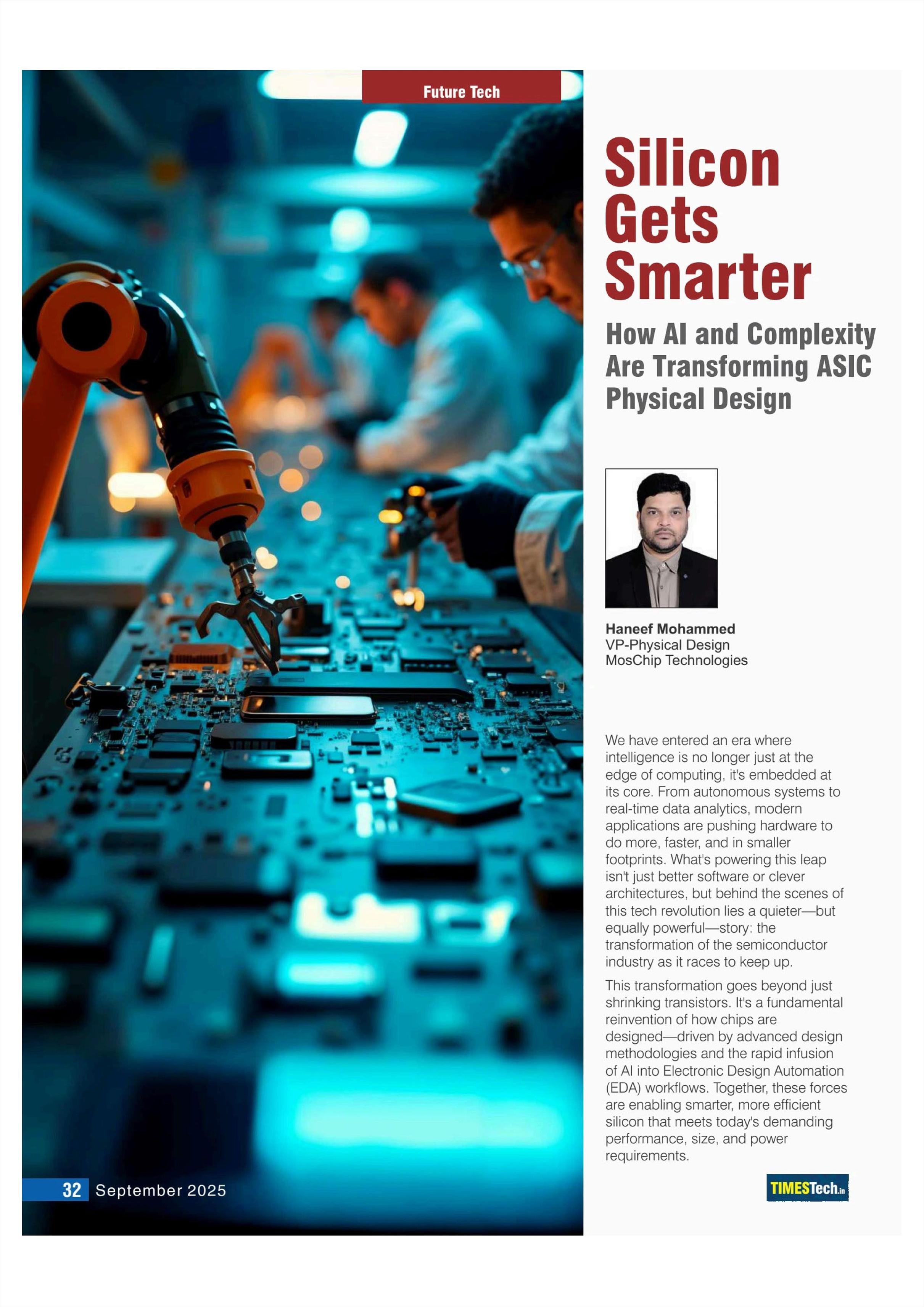
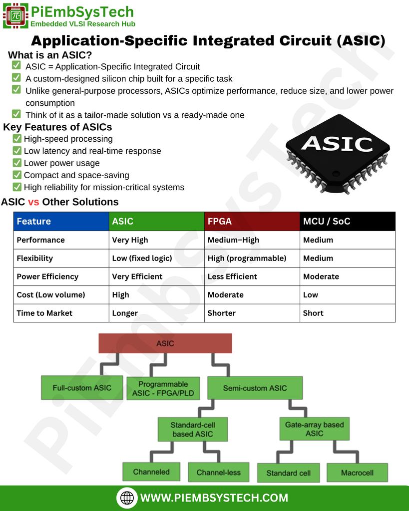
Almost three years ago, when I was still studying at university, I attended a lecture about the design of custom chips (ASICs) and I had the opportunity to design my own custom chip back then. Now, almost three years later I finally have the finished chip in front of me and can take some pictures of it :3

(It took a while before they put it in production, the actual desing only took about two months)

I'll have to wait until tomorrow to get access to a microscope to take photos of the actual chip, but here are some pictures taken in the design environment

Because I had to design the entire chip on my own and within a limited time frame, I chose something not too complicated for the design. The circuit is a 7-segment decoder for 4 different digits with an integrated counter and internal multiplexing

The entire chip is 1.9 mm high and 1.4 mm wide and was designed using a 350nm technology. The first image shows the entire chip (the inner logic surrounded by the IO ring with all the bond pads). The second picture shows the actual logic in close-up. Here you can see all the metal layers that connect everything together. I can't show you any of the silicon layers unfortunately e.g. where and how the silicon is doped and the polysilicon layer used for the transistor gates. Sharing this information is prohibited by the manufacturer of the chip (I had to sign a NDA).

I of course couldn't resist to add some furry art on the topmost metal layer :D

I used a script to convert every pixel of the original image into a metal square of a certain size and place it on the chip in the desing software. It was not easy to get the artwork design rule compliant, but with some manual rework I manged to do so ^^

The image on the chip is only roughly 700um high and 400um wide (0.7mmx0.4mm) (the slots in the scarf are necessary to comply with the desing rules), so it's probably one of the smallest physical furry artworks in existence x3

I really hope that I can take some good photos of the chip and the artwork tomorrow, but I'll have to see if the microscope has enough magnification

#electronics #asic #asicdesign

Picture of the whole chip. You can see the IO ring with the bond pads which surrounds the internal logic. On the right hand side is the artwork of my sona and at the bottom you can see the year it was designed. The white rectangle censors my legal name, which I also wrote on the chip.Close-up picture of the internal logic consisting of a shift register, four registers to store the individual numbers, a multiplexer, the seven segment logic, output drivers, a switch and a counter.Close-up picture of the artwork placed on the topmost metal layer. It's my sona waving at the viewer.
MosChip®MosChipTech
2025-09-18

Silicon Gets Smarter with AI in Physical Design.

In his feature with TimesTech, Haneef Mohammed (Our VP - Physical Design) shares how AI-powered EDA tools and advanced methodologies are redefining ASIC Physical Design

Adam Zhangdashthru
2025-08-19

Combine Tcl and Python in a single EDA Shell: tclpysh playground is now online.
dashthru.com/playground
( Use 'py' or 'tcl()' command to switch between languages )

2022-10-04

RT from Antmicro (@antmicro)

Join us at the Wroclaw Open Source Meetup Thursday 6.10, 6PM CEST and learn how #opensource tooling driven by @risc_v & @CHIPSAlliance, is democratizing #ASICdesign. 2nd talk dedicated to the ins and outs of #passwordless authentication w/ #OAuth2 & #OIDC. meetup.com/open-source-meetup-

Original tweet : twitter.com/antmicro/status/15

Client Info

Server: https://mastodon.social
Version: 2025.07
Repository: https://github.com/cyevgeniy/lmst