#camerasensor

2025-12-25

iPhone 18 Pro dự kiến sẽ sở hữu hệ thống camera đột phá nhờ công nghệ cảm biến hoàn toàn mới. Thay vì chỉ tập trung vào nâng cấp hiệu năng hay phần mềm, Apple hứa hẹn biến camera thành điểm nhấn lớn nhất trên dòng flagship tương lai này, mang lại chất lượng hình ảnh vượt trội.

#iPhone18Pro #Apple #TechNews #CameraSensor #iPhoneRumors #AppleVN #CongNghe #TinCongNghe #CameraiPhone

vietnamnet.vn/iphone-18-pro-se

I'm looking for a CMOS camera sensor for a FOSH project. I'm just looking for a surface mount chip without the lens.

It looks like two big brands are onsemi and omnivision. I've applied for NDA access to the datasheets, but I'm wondering if there are good options with open specs? How do people generally release FOSH based on chips with NDA specs?

I've gotten the OV7670 prototype boards configured using I2C and I can read frames out using the parallel interface.

Parallel interfaces are easy. Many cameras now have MIPI interfaces. Is it easy to read MIPI data? I am planning to use an FPGA to read the camera data, so although parallel would be easiest, I imagine there could be a MIPI Vertilog 2005 implementation that I could compile to run in my FPGA?

#foss #fosh #camera #sensor #camerasensor #fpga #mipi #onsemi #omnivision #cmossensor

Tony 💉x10 🇦🇺kongakong@masto.ai
2025-08-23

At f22, I can see some smudge in my photo images. Not sure if it is the lens or the sensor. I just cleaned the sensor a couple days ago. 😞

#camerasensor

Benjamin Carr, Ph.D. 👨🏻‍💻🧬BenjaminHCCarr@hachyderm.io
2024-02-07

#STMicroelectronics makes a 18K Big Sky #CameraSensor So Large Only Four on a 300mm Wafer
#BigSky is a custom 18K camera to shoot high-resolution video for the #MSG Sphere in #LasVegas. The team had to design not just the lenses and camera to capture video played in the Sphere. It also had to design the imaging sensor.
servethehome.com/stmicroelectr

Lowyat.NETlowyat
2023-11-21
petapixel (unofficial)petapixel@ծմակուտ.հայ
2021-12-16

Sony Unveils Groundbreaking CMOS Sensor That Gathers Twice the Light

Sony's Semiconductor division has announced that it successfully developed the world's first stacked CMOS image sensor technology with two-layer transistor pixels that grants double the light gathering capability.

Sony explains that typical image sensors place photodiodes and pixel transistors on the same substrate, but in this new design, it was able to separate them onto different substrate layers. The result is a sensor that approximately doubles the saturation signal level -- basically its light gathering capability -- which dramatically improves the dynamic range and reduces the noise

Saturation signal level isn't directly a sensor's light-gathering capability but is a major gating factor that influences how accurately a sensor is able to interpret light information in dim environments. For the sake of basic explanation, double the light gathering ability is the end result of this advancement.

Typical stacked CMOS sensors use a structure of a pixel chip made up of back-illuminated pixels stacked on top of a logic chip where signal processing circuits are formed. Within each chip, photodiodes that convert the light to electrical signals and pixel transistors that control the signals are situated next to each other on the same layer.

Stacked CMOS image sensor architectures.

Sony’s new architecture is an advancement in stacked CMOS image sensor technology that separates the photodiodes and pixel transistors onto separate substrates that are stacked on top of each other, rather than side-by-side. Sony says that the new stacking technology enables the adoption of architectures that allow the photodiode and pixel transistor layers to each be optimized, thereby approximately doubling saturation signal level relative to conventional image sensors and, in turn, widening dynamic range.

"Additionally, because pixel transistors other than transfer gates (TRG), including reset transistors (RST), select transistors (SEL) and amp transistors (AMP), occupy a photodiode-free layer, the amp transistors can be increased in size," Sony says. "By increasing amp transistor size, Sony succeeded in substantially reducing the noise to which nighttime and other dark-location images are prone."

The result for photography means wider dynamic range (better exposure in photos with harsh backlighting or in dim settings) and lower noise in photos that are taken in dark environments. Sony specifically notes that this technology is going to make for increasingly high-quality imaging in the case of smartphone photography. The new technology’s pixel structure will enable pixels to maintain or improve their existing properties at not only current but also smaller pixel sizes.

That last note is particularly important, as it signals that Sony believes it has found a way to markedly improve the photo quality of smartphone sensors. In short, the quality of mobile photography could very well see a huge leap in performance thanks to this breakthrough.

Sony doesn't specify when it plans to manufacture sensors at scale using this technology but does say it will continue to iterate on the design to further increase image quality in sensors large and small.

#equipment #news #technology #camerasensor #dynamicrange #groundbreaking #improvedphotos #lowlight #mobile #mobilephotography #newtech #sensortech #smallpixels #smartphone #smartphonecamera #smartphonesensor #stackedcmos

imageDiagram of stacked CMOS architecture
petapixel (unofficial)petapixel@ծմակուտ.հայ
2021-09-27

Teardown Shows iPhone 13 Pro Camera Module is Much Larger

The iPhone 13 series may look like an incremental update from the outside, but the team from iFixit shows that after a teardown, there are some notable differences from the 12 Pro series, especially when it comes to the camera.

The iFixit team reports that there are seven main upgrades between the iPhone 12 Pro and iPhone 13 Pro. Specifically, the iPhone 13 Pro features an A15 Bionic chip with a new 5-core GPU and 6-core CPU as well as a 16-core Neural Engine. It also has 6GB of RAM and a base 128GB of storage that is configurable up to 1 TB. It also has support for Sub-6 GHz (and mmWave on the US models), 4×4 MIMO LTE, 2×2 MIMO 802.11ax Wi-Fi 6, Bluetooth 5.0, Ultra Wideband, and NFC.

The display has also been upgraded and on the iPhone 13 Pro is a 6.1-inch (2532 × 1170 pixels) Super Retina XDR OLED display with ProMotion, which means the display can intelligently shift the refresh rate from very low all the way up to 120Hz. It also gets 15W wireless charging and IP68 water resistance.

But most notably for photographers, the camera array looks very different. The specifications sheet says it's a 12-megapixel triple camera system made up of an ultra-wide-angle (ƒ/1.8), wide-angle (ƒ/1.5), and 3x telephoto (ƒ/2.8) cameras, plus a LiDAR module. But the on-paper specifications don't really do the changes to this system justice.

In the photo above, iFixit shows that the iPhone 13 camera module (left) is much larger than the one found in the iPhone 12 Pro's array (right). Side by side, there is a clear difference.

But the iPhone 12 Pro did not have the most robust camera system of the last generation -- that went to the Pro Max. So how does the iPhone 13 Pro camera's size compare? Honestly, it's hard to say from the photos iFixit has provided since the organization did not take photos from the same angles of the two models. It looks similar, but there are definitely some differences. For example, Apple added stabilization to all three cameras on the iPhone 13 Pro, up from just one on the 12 Pro Max.

The photos below are from iFixit 's 2020 teardown of the iPhone 12 Pro Max:

On a related note, a report from GSMArena claims that the camera sensors in the 13 Pro series are completely different from the ones found in the 12 Pro Max. A Chinese enthusiast claims that all three have a new Sony IMX 7-series sensor behind them. The main camera is supposedly a Sony IMX703, the ultra-wide is apparently a Sony IMX772, and the telephoto is supposedly a Sony IMX713. The iPhone 12 Pro Max reportedly used Sony 6-series sensors.

As interesting as it is to see these modules outside of their home, the main reason iFixit performs its teardowns is to provide a repairability score to electronics. Last year, the iPhone 12 Pro Max scored a 6 out of 10 for repairability, and this year the iPhone 13 Pro scores a 5 out of 10. iFixit says that in addition to the glass back that made the iPhone 12 Pro Max difficult to repair, the iPhone 13 Pro software component pairing "needlessly complicates" many repairs.

iFixit 's full teardown of the iPhone 13 Pro can be seen on its website.

Image credits: All teardown images by iFixit.

#mobile #news #apple #camerasensor #ifixit #iphone #iphone12pro #iphone12promax #iphone13 #iphone13pro #iphone13promax #iphonecamera #smartphonecamera #teardown

image
petapixel (unofficial)petapixel@ծմակուտ.հայ
2021-09-10

Why Camera Sensors Matter and How They Keep Improving

What is the most important aspect of a camera to consider when looking to buy a new one? In this video, Engadget put camera sensors in the spotlight and reviewed how they have improved and what role they play in today's photographic equipment.

Camera brands regularly release new cameras, with each model improving on its past versions. However, video producer Chris Schodt from Engadgetpoints out in the company's latest YouTube video that it may appear camera sensors haven't progressed as rapidly in the recent past, although resolution has increased. This is because modern-day cameras -- such as the Canon EOS 5D released in 2005 -- were already able to produce high-quality images over a decade ago and still continue to do so.

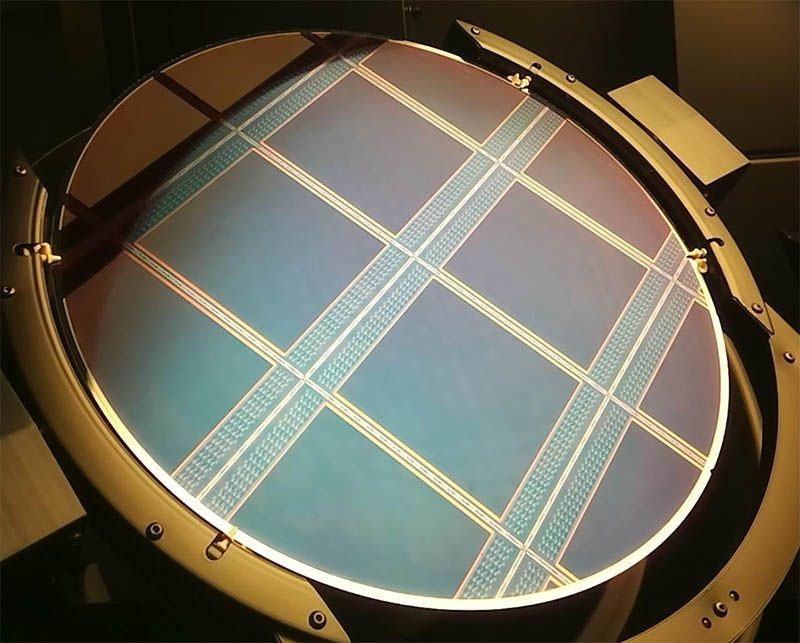
Camera sensors, in technical terms, can be described as a grid of photodiodes which act as a one-way valve for electrons. In CMOS sensors -- which are widely used in digital cameras that photographers use today -- each pixel has additional circuitry built into it aside from the photodiode.

These on-pixel electronics help CMOS sensors quick speed because they can read and reset quickly, although, in the past, this characteristic could also contribute to bringing up fixed-pattern noise. However, with the improvement of manufacturing processes, this side-effect has been largely eliminated in modern cameras.

Schodt explains that noise control is crucial to a camera's low light performance and dynamic range, which is a measure of the range of light captured in the image between the maximum and minimum values. In a photograph, those are between white -- such as when pixel clips or is overexposed -- and black, respectively.

Clipped or overexposed pixels in an image

In an ideal scenario, camera sensors would capture light, which is emitted as photons, in a uniform way to reconstruct a perfectly clear image. However, that isn't the case because they hit the sensor randomly.

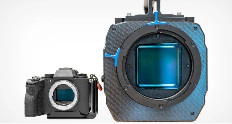
One way to deal with this is to produce larger sensors and larger pixels, however, that comes with a large production cost and an equally large camera body, such as the Hasselblad H6D-100c digital back which has a 100MP CMOS sensor and a $26,500 price.

Other solutions include the development of Backside Illuminated sensors (BSI), such as the one announced by Nikon in 2017 and Sony first in 2015. This type of sensor leads to improved low-light performance and speed. Similarly, so does a stacked CMOS sensor that provides even faster speeds, such as the Sony Micro Four Thirds sensor published earlier in 2021.

Smartphones, on the other hand, use multiple images and average them together to improve noise and dynamic range, like the Google HDR+ with Bracketing Technology, which is also a direction that several modern video cameras have taken, too.

Looking towards the future of sensor development, Schodt explains that silicon, which is the material currently used to make sensors, is likely to stay, although some alternative materials have been used like gallium arsenide and graphene. Another possible direction is curved sensors, although they would make it difficult for users as curved sensors would need to be paired with precisely manufactured lenses. In practical terms, photographers would have to buy into a particular system with no option of using a third-party lens.

It's likely that in the future focus will be on computational photography. Faster sensors and more on-camera processing to make use of smartphone-style image stacking might make its way to dedicated cameras, for example, in addition to AI-advanced image processing.

In the video above, Schodt explains more in detail the technical build of sensors and how their characteristics correlate to the resulting images. More Engadget educational videos can be found on the company's YouTube page.

Image credits: Photos of camera sensors licensed via Depositphotos.

#educational #technology #backsideilluminated #bsi #camerasensor #cmos #cmossensor #curvedsensor #digitalbacks #engadget #sensor #smartphonecamerasensor

image
petapixel (unofficial)petapixel@ծմակուտ.հայ
2021-08-02

Sony Officially Warns That Lasers Can Damage its Cameras’ Sensors

Sony has published an official warning on its website that states that it is aware that lasers can cause damage to its cameras' image sensors. While this information is probably not news to most, Sony notably has finally publicly acknowledged the danger.

While there have been stories that report the damage that lasers can cause to camera sensors that date as far back as 2010, Sony has chosen to officially note the problem on its website just in this past week. Spotted by Image Sensors World and published on July 30, 2021, Sony answers the question "can the camera image sensor be damaged by laser?"

Do not directly expose the Lens to beams such as laser beams. This may cause damage to the image sensor and cause the camera to malfunction.

Note: In either outdoor or indoor environment when there is a laser display, tendency of direct or indirect (laser beam bounce from reflective object) damage to the camera CMOS Sensor is still very high.

There has been no shortage over the years of instances where users have reported sensor damage that appeared linked to exposure to a variety of lasers. In 2010, a video shows how a Canon 5D Mark II DSLR responded when laser lights at a concert shined directly on his camera's sensor.

In 2013, a similar situation occurred at another concert, but this time it seriously damaged a $20,000 RED Epic. 2019 was a particularly eventful year for sensor destruction via laser, as both a self-driving car laser and a tattoo laser were the culprits behind two destroyed sensors. Additionally, Hong Kong pro-democracy protesters were using laser pointers to confuse and destroy surveillance cameras being used against them.

In the first instance, a man attending the Consumer Electronics Show (CES) in Las Vegas says that a car-mounted LIDAR permanently damaged the sensor in his Sony Alpha 7R Mark II camera. At the time, PetaPixel 's DL Cade reported that different lidar systems feature different designs and lasers, so many or most of them may be completely safe for cameras. It was unfortunate that in this particular case, it appeared the laser permanently damaged the camera's sensor.

In the second instance, a video shows a tattoo removal laser destroying pixels on a Sony Alpha 7S camera sensor.

“Don’t record laser tattoo removal on… anything,” the unlucky photography said at the time. “You can see with each pulse the sensor shows new damage. The repair cost was about as much as a new camera so try to avoid this.

Finally, PetaPixel 's Michael Zhang reported that during the protests in Hong Kong in 2019, demonstrators widely used handheld laser pointers in their anti-government demonstrations, and some photographers on the ground reported damaged sensors after their cameras were exposed to them.

So while there has been over a decade's worth of instances that show lasers can destroy camera sensors, it is somewhat notable that a camera company has finally published some admission of the issue. Hopefully, this will help photographers keep their equipment safe.

Image credits: Header photo licensed via Depositphotos.

#equipment #news #camerasensor #cmos #damage #destroyed #laser #official #sensor #sony #sonycameras #sonywarning

image

Client Info

Server: https://mastodon.social
Version: 2025.07
Repository: https://github.com/cyevgeniy/lmst