BCNC secures first overseas order for semiconductor polysilicon products, marking successful quality verification and plans for mass production supply to North American market
#YonhapInfomax #BCNC #Polysilicon #Semiconductor #NorthAmericanMarket #QualityVerification #Economics #FinancialMarkets #Banking #Securities #Bonds #StockMarket
https://en.infomaxai.com/news/articleView.html?idxno=50259
#polysilicon
Proposed polysilicon plant using Queensland sand seeks government approval.
The plant will supply polysilicon, the key raw material in the solar photovoltaic (PV) supply chain and metallurgical silicon, the key raw material in computer chip supply chain.”
Quinbrook has added a huge 750 MW battery to the plant design
#Queensland #Townsville #Australia #PV #Energy #FarNorthQld #Solar #Silicon #polysilicon #Computerchips #computers
Indian solar panels face US scrutiny for possible links to China forced labour
https://www.scmp.com/news/asia/south-asia/article/3276133/indian-solar-panels-face-us-scrutiny-possible-links-china-forced-labour?utm_source=rss_feed #Uygur #forcedLabor #india #china #polysilicon #SolarPanels
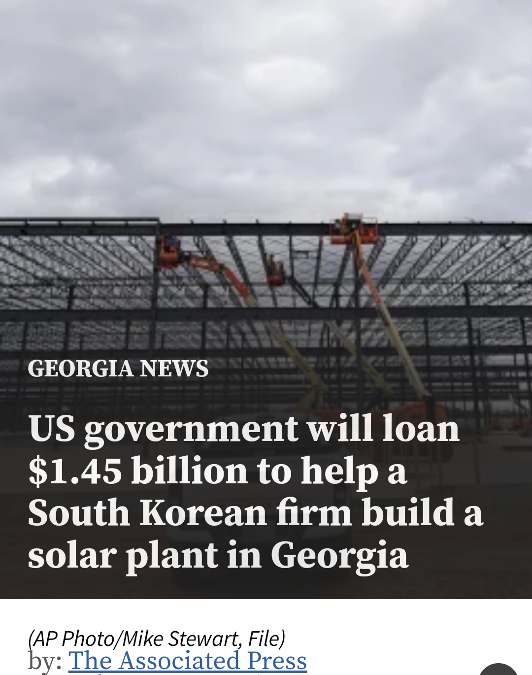
#Taxpayers #LetTheSunshineIn : U.S. #DOE grant expected to fund majority of $2.2 billion complex for #Qcells (division of #SouthKorean #Hanwha Group) to build a solar plant in #Georgia.
President Joe #Biden’s #InflationReductionAct, gives tax credits on #AmericanMade solar gear, plus allows manufacturers to earn #incentives for every unit of #polysilicon they refine in every wafer, cell and module they make in #USA.
A US Dept of #Energy spokesman said “The domestic demand for #solar modules in 2026 is expected to be around 50 #gigawatts. We’re expecting to produce about 40 gigawatts in 2026, So that means 80% of the (#solarpower) modules that we deploy in the United States in 2026 is expected to be domestic.”
After screwing around and holding cargo for 12+ months, U.S. Customs is now excluding #solar panels (modules) made by a certain module maker using polysilicon from the world's largest poly maker: Tongwei.
While we believe that this exclusion so far only applies to one module maker, it means that no modules using Tongwei poly are safe to import; ultimately no Chinese poly is safe to import.
China had 86% of global #polysilicon production at last count. /1
“Daqo starts operations of its #polysilicon production capacity of 100,000 MT in Inner Mongolia. The construction of the phase I took 10 months to complete. “
Much faster than in thought to deploy polysilicon.
Silicon cost per watt down 96% over last two decades
Since 2004, the volume of polysilicon per watt is down by 87%, and the...
Article Source: https://pv-magazine-usa.com/2023/01/10/silicon-cost-per-watt-down-96-over-last-two-decades/
#renewable, #markets, #policy, #semiconductor, #polysilicon, #pv, #semic
“Although the latest slump of the #polysilicon #price is pretty heavy (concurrently with that of #wafers), it will likely come to a halt in the second half of January when customers replenish their inventories ahead of the Chinese New Year holidays.
After that, we could even see a short-term price rebound if #demand grows more rapidly than #supply in the first half of 2023.”
REC Silicon partners with Ferroglobe as US polysilicon supply chain plans take shape
REC Silicon will negotiate a raw material supply agreement with silico...
Article Source: https://www.pv-tech.org/rec-silicon-partners-with-ferroglobe-as-us-polysilicon-supply-chain-plans-take-shape/
#fbr, #silicon, #sema, #polysilicon, #rec, #ferroglobe, #production, #news
Daqo fires up 35,000-ton poly fab
The polysilicon producer is sticking by plans to ramp up manufacturing...
Article Source: https://www.pv-magazine.com/2021/12/08/daqo-fires-up-35000-ton-poly-fab/
#modules, #glut, #n-type, #upstream, #daqo, #manufacturing, #polysilicon
Mining and Refining: Pure Silicon and the Incredible Effort It Takes to Get There
Were it not for the thin sheath of water and carbon-based life covering it, our home planet would perhaps be best known as the "Silicon World." More than a quarter of the mass of the Earth's crust is silicon, and together with oxygen, the silicate minerals form about 90% of the thin shell of rock that floats on the Earth's mantle. Silicon is the bedrock of our world, and it's literally as common as dirt.
But just because we have a lot of it doesn't mean we have much of it in its pure form. And it's only in its purest form that silicon becomes the stuff that brought our world into the Information Age. Elemental silicon is very rare, though, and so getting appreciable amounts of the metalloid that's pure enough to be useful requires some pretty energy- and resource-intensive mining and refining operations. These operations use some pretty interesting chemistry and a few neat tricks, and when scaled up to industrial levels, they pose unique challenges that require some pretty clever engineering to deal with.
Hard as Rock
The raw material for most silicon production is the mineral quartzite. Quartzite comes from ancient deposits of quartz sands that formed sedimentary deposits. Over time and with heat and pressure, these quartz sandstones were transformed into the metamorphic rock quartzite, which is at least 80% quartz by volume.
Quartzite. Source: Geology.com
Quartzite is an incredibly tough rock, and where it pokes above the surface, it forms ridges that strongly resist weathering. Significant formations of quartzite are scattered all around the world, but there are relatively few places where it makes financial sense to quarry the rock for silicon production, since the formations need to be easily accessible and relatively close to the other raw materials and energy supply needed.
Raw quartzite is mostly silicon dioxide (SiO2), and the refining process begins with a reduction reaction to get rid of the oxygen. Crushed quartzite is mixed with carbon in the form of coke (coal that has been heated in the absence of oxygen). Woodchips are added to the charge as well; they serve both as a carbon source and a physical bulking agent that allows gasses and heat to circulate better in the furnace.
The arc furnaces for silicon smelting are massive installations with huge carbon electrodes. The electrodes are consumed during smelting, so new electrodes are screwed onto the tops of the current electrodes to make sure the process isn't interrupted. The arc furnace requires massive amounts of electricity to maintain the 2,000°C temperature needed, so silicon refineries are often located where electricity is cheap and plentiful.
The reduction reactions inside the melt zone are actually pretty complicated, but can be summed up with two main reactions:
In both reactions, the oxygen in the silicon dioxide combines with carbon to form the main waste product, carbon monoxide. A side reaction that occurs in a part of the melt zone inside the furnace produces silicon carbide (SiC), which is an unwanted byproduct (at least when the goal is to purify silicon; silicon carbide itself is a useful industrial abrasive). By making sure that silicon dioxide is far in excess in the furnace, the second reaction where the SiC acts as a carbon source for the reduction of silicon dioxide is favored, and silicon with up to 99% purity can be tapped off the bottom of the furnace.
The silicon produced by this process is referred to as metallurgical silicon. For almost all industrial uses, this highly purified silicon is good enough. About 70% of metallurgical silicon goes to the manufacture of metal alloys such as ferrosilicon as well as aluminum-silicon, an alloy that contracts minimally upon cooling and is therefore used to cast aluminum engine blocks and similar items.
More Nines
Monosilane is the silicon equivalent of methane. In trichlorosilane, three of the hydrogens are substituted for chlorines. Source: WebElements
As useful as metallurgical silicon is, even at 99% pure it's not even close to the purity needed for semiconductor and photovoltaic applications. The next steps in purification take the silicon to the purity level that's needed for semiconductor manufacture. Purification starts by mixing powdered metallurgical silicon with hot, gaseous hydrochloric acid. This reaction produces silanes, which are compounds with a central silicon atom surrounded by four attachments, in this case three chlorine atoms and one hydrogen. This trichlorosilane is a gas at the temperature inside the reaction chamber, which makes it easier to handle and purify by fractional distillation.
When the trichlorosilane gas has been sufficiently purified, polycrystalline silicon production can begin. The Siemens process is the main method here, and is a form of chemical vapor deposition. A large bell-shaped reaction chamber contains several thin threads of highly purified silicon, which are heated to 1,150°C by passing an electric current through them. A mixture of gaseous trichlorosilane and hydrogen flows into the chamber; the gas decomposes on the hot electrode leaving behind the silicon, which accretes into rods that are about 15 cm in diameter. Polycrystalline silicon made by the Siemens process can have a purity of 99.99999% ("seven nines", or 7N) or more. 7N to 10N polysilicon is mostly used for photovoltaic cells, although some polysilicon in this purity range also makes it into MOSFET and CMOS semiconductors.
Polysilicon rods from a Siemens process chamber. Source: Silicon Products Group GmbH
While the Siemens process is the polysilicon workhorse, it has its disadvantages. The main problem is that it's an energy hog -- keeping the growing polycrystalline rods hot enough to decompose the feedstock requires a lot of electricity. To work around this problem, a fluidized bed reactor (FBR) process is sometimes used. An FBR reactor is shaped like a tall tower, the walls of which are lined with a quartz tube. Silane gas, either the familiar trichlorosilane or monosilane, which is just a silicon atom surrounded by four hydrogens, is injected into the chamber. Powdered silicon is dropped into the reaction chamber from the top, while heated hydrogen gas is injected into the bottom of the chamber through a series of nozzles. The gas flow keeps the hot silicon powder fluidized, allowing it to mix with the silane gas and decompose it. As in the Siemens process, the silicon accretes onto the seed particles, which eventually get too large for the fluidized bed to support. The polycrystalline silicon beads drop to the bottom of the chamber, where they can be collected.
Aside from power savings -- up to 90% less when using monosilane as a feedstock -- the FBR method's main advantage is that it's a continuous process, since the finished beads can just be pumped out of the chamber. The Siemens process is more of a batch process, since the reactor chamber has to be opened to remove the polysilicon rods when they're finished. That said, FBR polysilicon hasn't really taken off, in part because managing the fluid dynamics inside the reaction chamber can be difficult. But the main reason is that the Siemens process is just so easy, and as long as factories can be located near a source of cheap electricity, it's just easier to use the brute-force method.
Polysilicon production by the Siemens process and fluidized bed reactor. Source: Bernreuter Research
One Crystal Only, Please
Using either of these methods, polycrystalline silicon can be brought to extremely high purity, up to 11N. But purity isn't the only metric for silicon; sometimes, the nature of the crystalline structure on the end product is just as important as purity. The next step in silicon production is the creation of monocrystalline silicon, where the entire silicon ingot is a single crystal.
Growing a single crystal of ultra-pure silicon to a size that's industrially useful is no mean feat, and relies on some tricks discovered in 1916 by Polish chemist Jan Czochralski. We've covered the Czochralski method in depth before, but briefly, polycrystalline silicon is melted in a quartz crucible in an inert atmosphere. A puller rod bearing a single ultra-pure silicon crystal that is very precisely oriented is lowered into the molten silicon. The seed crystal causes silicon to condense, continuing the crystal structure as the puller rod is slowly withdrawn from the furnace while rotating. Single-crystal ingots up to 450 mm in diameter are possible with the Czochralski method.
Another method to produce monocrystalline silicon is the float zone method, which uses a polycrystalline silicon rod as the starting material. Inside a reaction chamber with an inert gas atmosphere, a radio frequency signal is passed through a coil that surrounds the rod. The RF signal heats the polysilicon, creating a confined melt zone. Single crystals of ultra-pure silicon are added to the melt zone, which causes the molten silicon to crystallize around it. The RF coil is slowly moved up the rod, moving the zone of heating until the entire rod is a single crystal of silicon. Float-zone monocrystalline silicon has the advantage of never being in contact with the quartz walls of the Czochralski method crucible, and so will have less contamination from oxygen and other impurities.
#chemistryhacks #engineering #featured #originalart #science #crystal #metallurgy #miningandrefining #polysilicon #quartz #quartzite #silane #silicon #silicondioxide
PODCAST: What should solar expect from COP26, pricing woes dent renewables prospects
Global renewables industries are expectant as COP26 looms, however sup...
Article Source: https://www.pv-tech.org/podcast-what-should-solar-expect-from-cop26-pricing-woes-dent-renewables-prospects/
#storage, #news, #solar, #cop26, #ipo, #polysilicon, #m&a, #podcast
US solar companies call for caution and clarity as trade barriers mount
US solar companies have called upon the Biden administration to excise...
Article Source: https://www.pv-tech.org/us-solar-companies-call-for-caution-and-clarity-as-trade-barriers-mount/
#policy, #polysilicon, #biden, #anti, #regulation, #news, #dumping, #president
When someone offers to write you a check for $5 billion for your company, it seems like a good idea to take it. But in the world of corporate acquisitions and mergers, that's not always the case, as Altium proved this week when they rebuffed a A$38.50 per share offer from Autodesk. Altium Ltd., the Australian company whose flagship Altium Designer suite is used by PCB and electronic designers around the world, said that the Autodesk offer "significantly undervalues" Altium, despite the fact that it represents a 42% premium of the company's share price at the end of last week. Altium's rejection doesn't close the door on ha deal with Autodesk, or any other comers who present a better offer, which means that whatever happens, changes are likely in the EDA world soon.
There were reports this week of a massive explosion and fire at a Chinese polysilicon plant -- sort of. A number of cell phone videos have popped up on YouTube and elsewhere that purport to show the dramatic events unfolding at a plant in Xinjiang province, with one trade publication for the photovoltaic industry reporting that it happened at the Hoshine Silicon "997 siloxane" packing facility. They further reported that the fire was brought under control after about ten hours of effort by firefighters, and that the cause is under investigation. The odd thing is that we can't find a single mention of the incident in any of the mainstream media outlets, even five full days after it purportedly happened. We'd have figured the media would have been all over this, and linking it to the ongoing semiconductor shortage, perhaps erroneously since the damage appears to be limited to organic silicone production as opposed to metallic silicon. But the company does supply something like 17% of the world's supply of silicon metal, so anything that could potentially disrupt that should be pretty big news.
It's always fun to see "one of our own" take a project from idea to product, and we like to celebrate such successes when they come along. And so it was great to see the battery-free bicycle tire pressure sensor that Hackaday.io user CaptMcAllister has been working on make it to the crowdfunding stage. The sensor is dubbed the PSIcle, and it attaches directly to the valve stem on a bike tire. The 5-gram sensor has an NFC chip, a MEMS pressure sensor, and a loop antenna. The neat thing about this is the injection molding process, which basically pots the electronics in EDPM while leaving a cavity for the air to reach the sensor. The whole thing is powered by the NFC radio in a smartphone, so you just hold your phone up to the sensor to get a reading. Check out the Kickstarter for more details, and congratulations to CaptMcAllister!
We're saddened to learn of the passing of Dale Heatherington last week. While the name might not ring a bell, the name of his business partner Dennis Hayes probably does, as together they founded Hayes Microcomputer Products, makers of the world's first modems specifically for the personal computer market. Dale was the technical guru of the partnership, and it's said that he's the one who came up with the famous "AT-command set". Heatherington only stayed with Hayes for seven years or so before taking his a $20 million share of the company and retiring, which of course meant more time and resources to devote to tinkering with everything from ham radio to battle bots. ATH0, Dale.
#hackadaycolumns #hackadaylinks #altium #atcommand #autodesk #eda #hayes #kickstarer #mems #modem #nfc #polysilicon #sensor #siloxane
Daqo New Energy revenues inch up as surging polysilicon ASPs expected for next quarter
Major polysilicon provider Daqo New Energy has reported a rise in reve...
Article Source: https://www.pv-tech.org/daqo-new-energy-revenues-inch-up-as-surging-polysilicon-asps-expected-for-next-quarter/
#news, #new, #manufacturing, #polysilicon, #materials, #investment, #daqo, #energy
Client Info
Server: https://mastodon.social
Version: 2025.04
Repository: https://github.com/cyevgeniy/lmst