EuroRack 6HP MCU Experimenter Module Usage Notes
Here are some suggestions and usage notes for my EuroRack 6HP MCU Experimenter PCB.
This post walks through the different sections of the schematic and PCB and shows how to tailor the circuits to different applications.
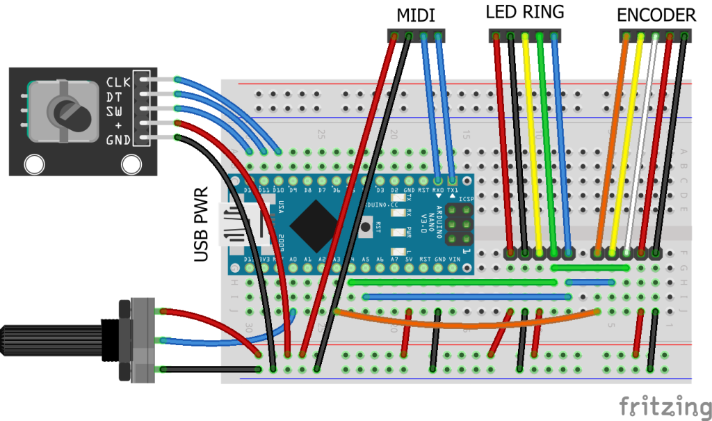
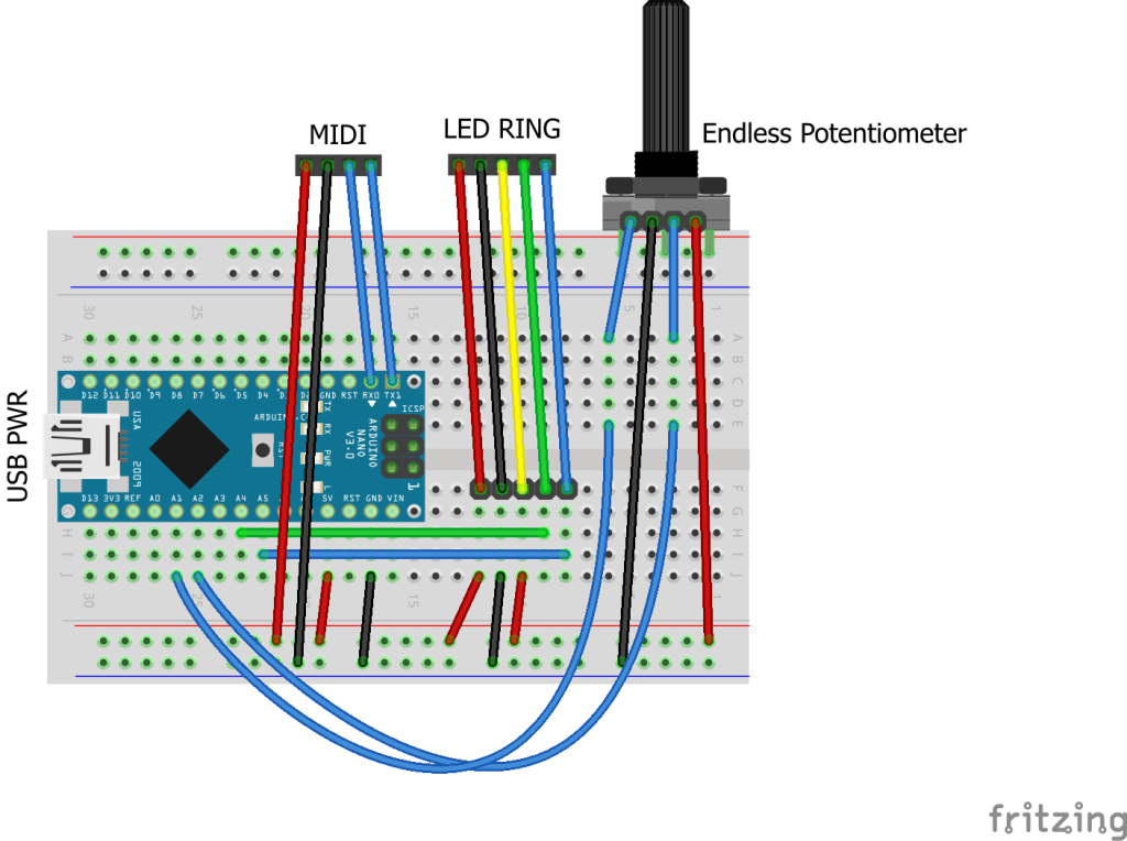
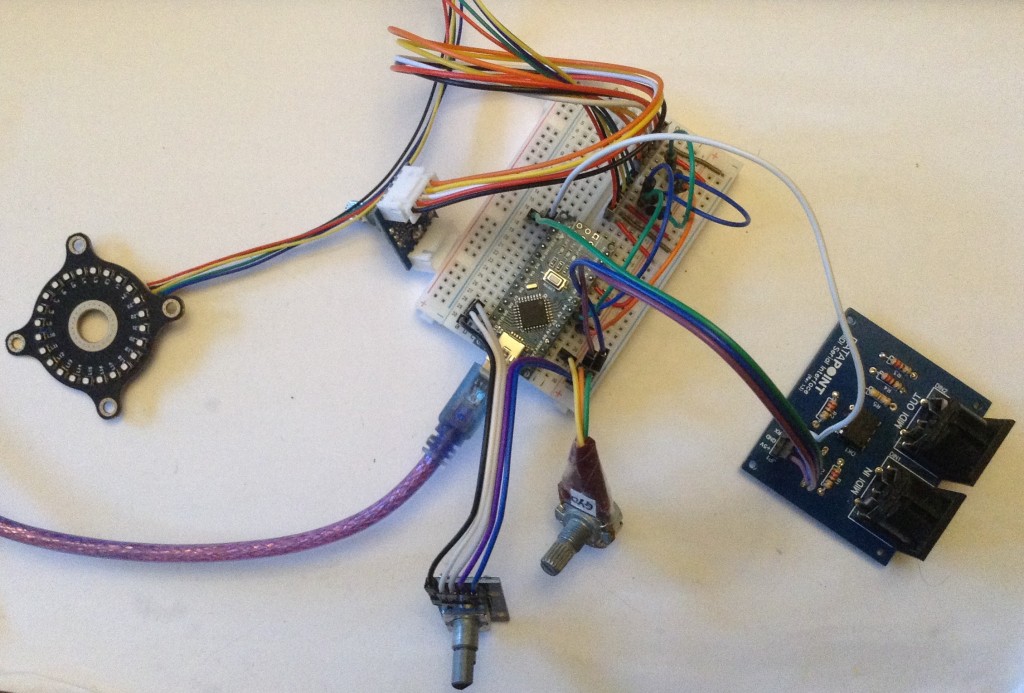
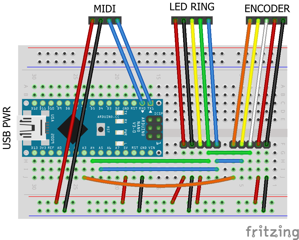
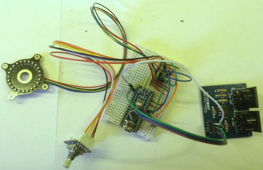
Here is a list of built modules using these boards:
Warning! These boards are meant for DIY systems only. They should NOT be used with expensive EuroRack modules, racks, or power supplies. I strongly recommend using old or second hand equipment for your experiments. I am not responsible for any damage to expensive instruments!
If you are new to Electronics, see the Getting Started pages.
Introduction
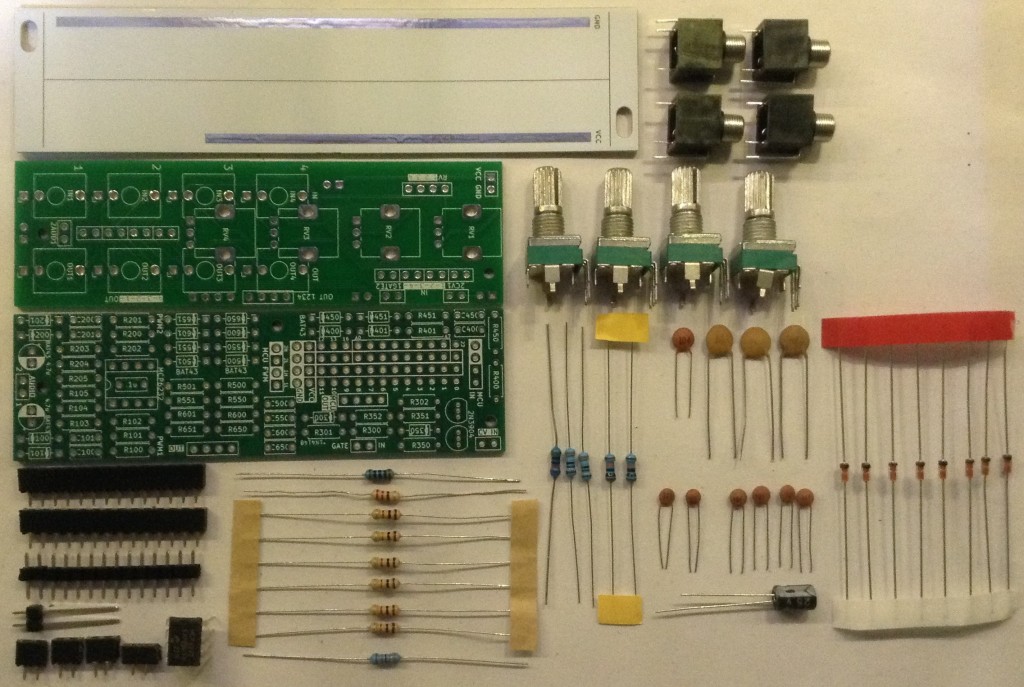
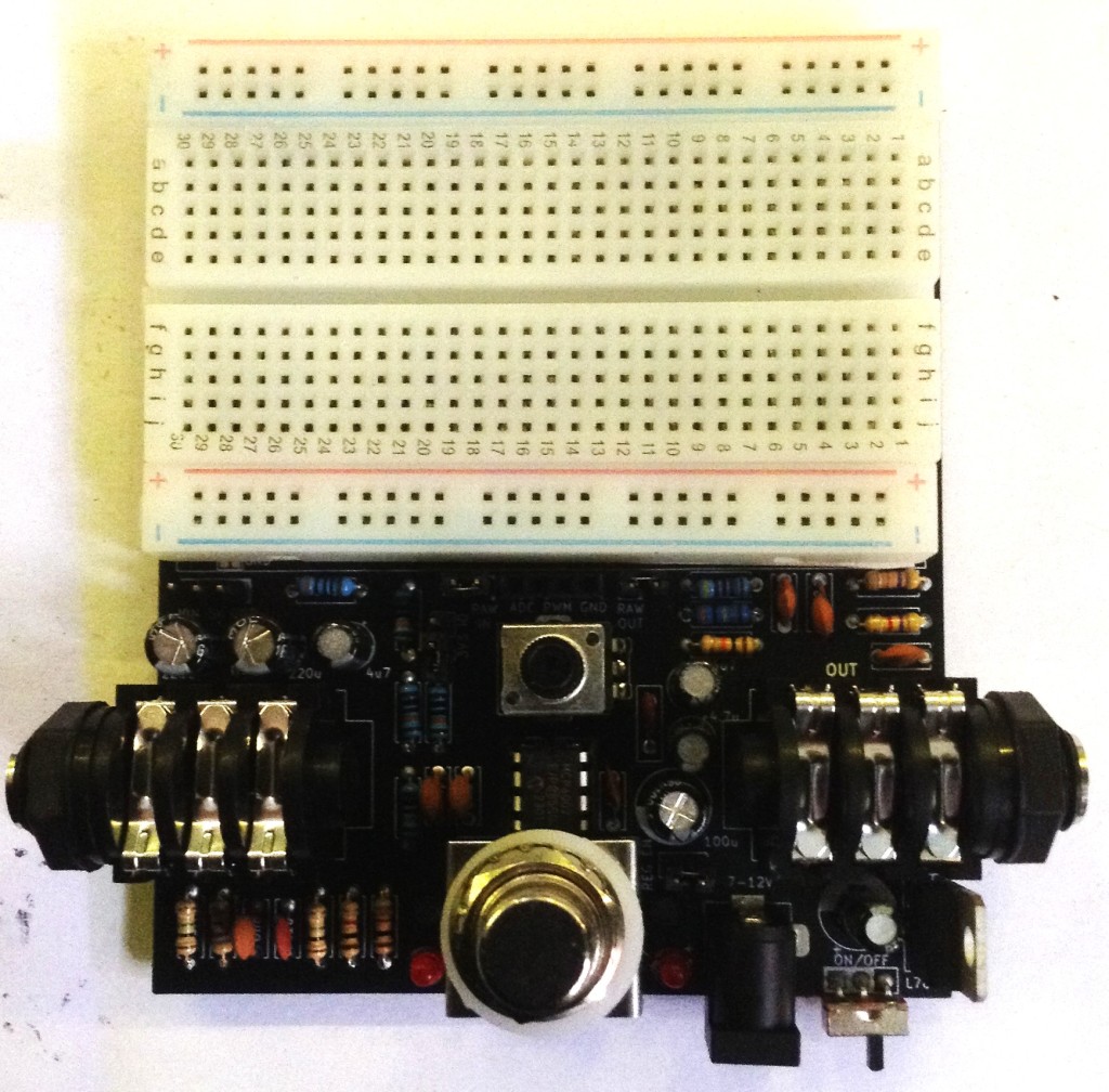
As detailed in the design notes, there are a number of different sections for this PCB, each designed to be used to link a microcontroller to a EuroRack synth in a useful, and hopefully electrically useful way. There is also an additional PCB designed to support a range of configurations of Pots and Jacks for use with this MCU and IO board.
At various points, I refer back to a range of HAGIWO’s designs in the discussion (for a complete list see my design notes).
But I have to reiterate right at the start – I strongly state that you DO NOT use these in a rack of expensive or cherished gear!
It is meant for DIY experiments and so it should be expected that:
- Use of this PCB could easily destroy any power supply powering it.
- Use of this PCB could also easily destroy any EuroRack modules in the same rack using the same power bus.
In short, I’m only using this with cheap, second hand, other DIY kit, or equally sacrificial equipment and I strongly state that you should do the same.
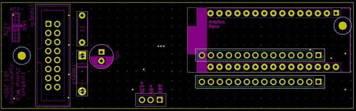
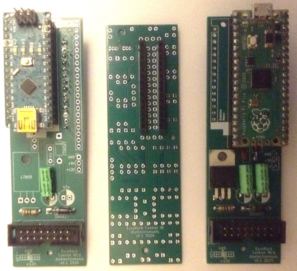
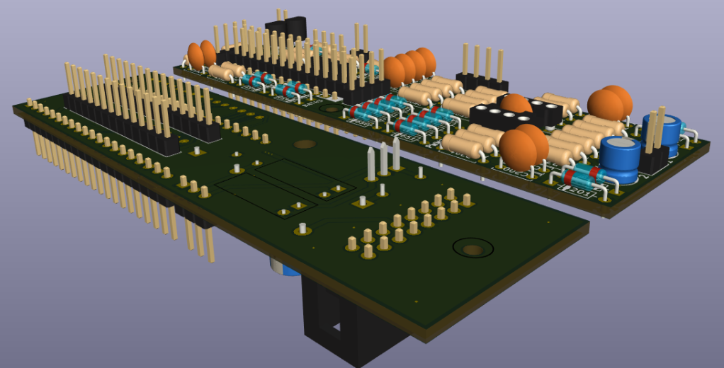
The Microcontroller Board
Recall that there are two PCBs to be used: an IO board and a MCU board. The MCU board could support either a Raspberry Pi Pico (or similar) or an Arduino Nano (or similar).
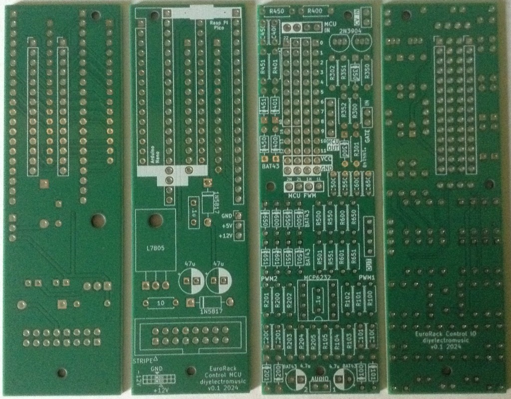
The MCU board has all of the components on the underside, apart from the two rows of headers joining it to the IO board. The IO board has all components on the top-side, apart from the two rows of headers joining it to the MCU board.
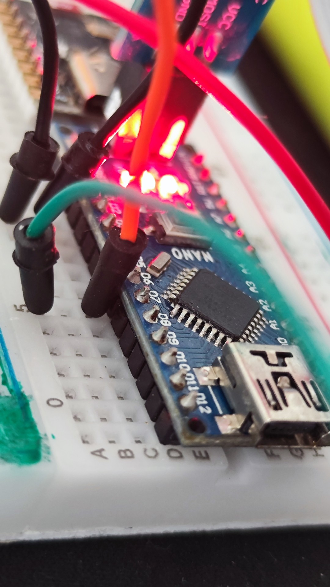
Arduino Nano
The following illustrate which components are required to use an Arduino Nano. This shows the rear view of the MCU board.
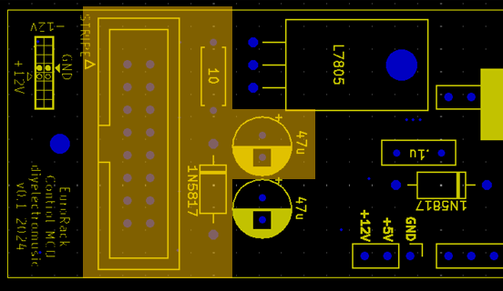
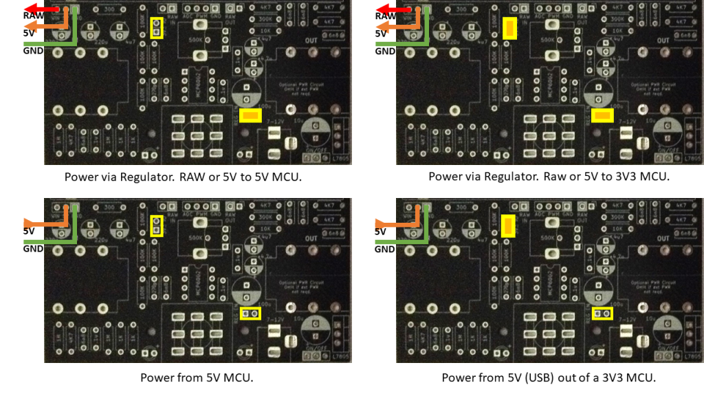
The Arduino Nano will run directly off the EuroRack +12V line, so no regulator or associated components are required. The following detail shows which components need to be mounted to support the Nano’s power.
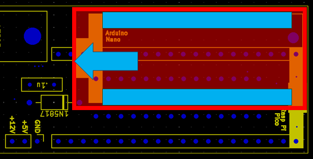
The Nano itself should be mounted on the two 15-way header sockets and aligned as shown below. Note that the USB connection is facing “down” towards the EuroRack power connector.
If the regulator and additional circuitry is already fitted it will be ignored if an Arduino Nano is used.
Raspberry Pi Pico
To use a Raspberry Pi Pico, the full power circuit is required, including the regulator, additional capacitors and diode as shown below. Once again this is showing the rear of the MCU board where all of the components (apart from the interconnecting headers) will be mounted.
The Pico will be mounted on the two 20-way header sockets and aligned as shown below, with the USB connector at the “top” facing away from the EuroRack power connector.
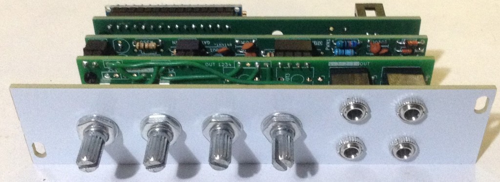
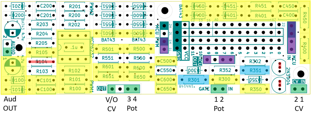
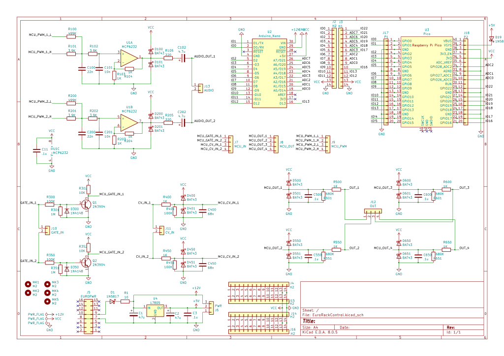
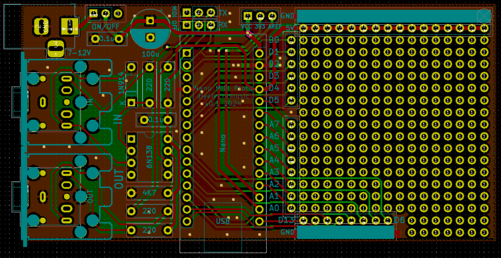
The IO Board
MCU Interface
The IO board itself will be connected to the microcontroller board using the interconnecting 14-way headers and all microcontroller IO pins will be broken out to pads as shown below.
The idea is that the main circuit sections terminate at one of the three MCU PWM|OUT|IN headers (also highlighted) and can then be patched across to the MCU IO headers which have the following layout.
GNDVCCD12D13(no)
D16A0A1A2A3
D17A4
D18A5
D19A6
D20A7
D21D22GNDVCCD11D10D9D8D7D6D5D4D3D2D1D0
The Arduino supports D0-D13 and A0-A7, although for an Arduino Nano A0-A6 can also be referenced as D14-D19 of course.
The Raspberry Pi Pico supports D0-D13, D16-D22 and A0-A2.
External Connections
Potentiometers, switches, jacks, audio or any other external IO can be connected to the IO board in a number of places. The following shows where they are and how they related to the MCU connections (assuming the appropriate circuitry in between has been connected up).
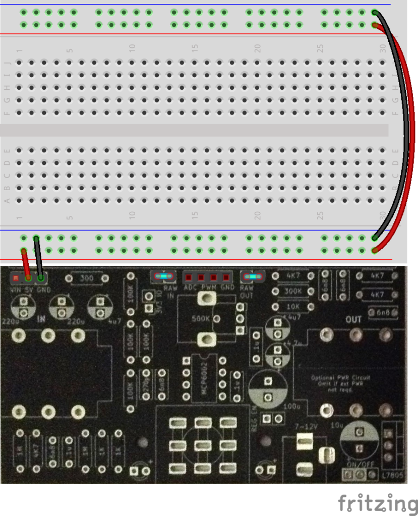
My additional Pots and Jacks PCB has been designed to match up with these headers and just needs a link to VCC and GND adding.
Which headers to use and how to do this is fully described in the Pots and Jacks PCB Build Guide.
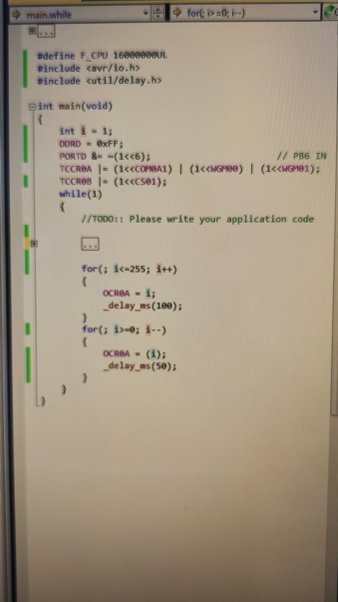
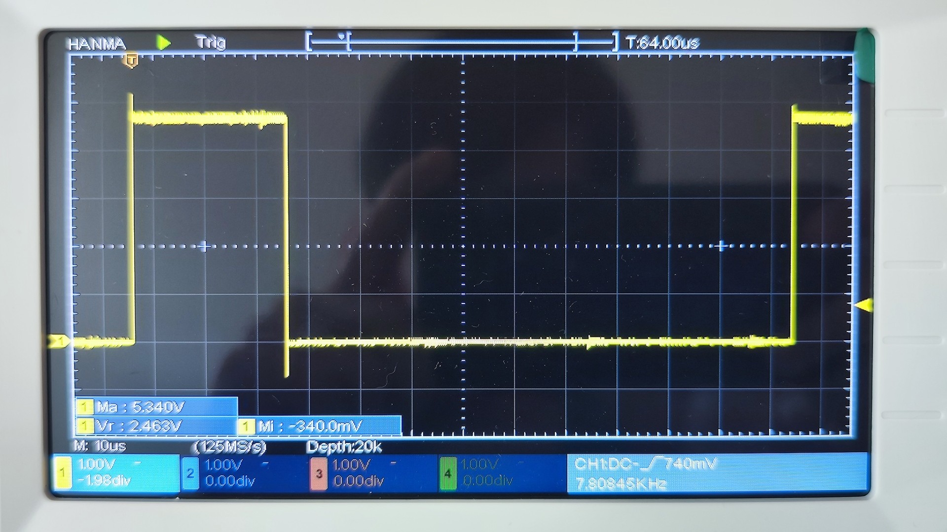
Audio PWM Output
There are two PWM output channels, each of which can be driven by one or two PWM outputs from the microcontroller. A great explanation of dual PWM output can be found on Open Music Labs here:
PWM Resolution and Filter
The PCB will support a single PWM output by omitting R100. If dual PWM output is required, then R100 and R101 need to have values that support the required bit-depth of the PWM resolution as described in the Open Music Labs tutorial (see “table 2”).
Some options might be:
SourceR100R101Resistor RatioPWM Resolution
Mozzi Dual499K3K9128Dual 7-bit
Proto Pedal PCB300K4K764Dual 6 bit
Otherwise a single resistor (e.g. R100) could be used for a single, 8-bit resolution PWM, in which case the chosen resistor will form part of the PWM filter consisting of R100 and C100.
As shown, there is a two-stage PWM filter circuit: R100/R101 and C100; R102 and C101. For a simpler application the second stage could be omitted and R102 replaced with a wire link (or short, for 0K).
In HAGIWO’s Nano design, the first stage uses values as per the Mozzi dual PWM default (above) with a 4n7 capacitor. The second stage uses a second 3K9 resistor with a 10nF capacitor. In the XIAO DAC application, HAGIWO uses a single resistor output from the DAC with a two stage filter of twin 10K + 1nF.
From the Open Music Labs tutorial, we have the following relationships for dual PWM and a low-pass filter:
- R2 = R1 . 2^n
- C ~= 1 / ( 2 . pi . R1 . Fc)
So the cutoff frequency Fc = 1 / ( 2 . pi . R1 . C ) where R1 is the smaller of the two resistors, so R101.
But when there are two filter stages, the RC calculation seems to be quite a bit more complicated and beyond my current knowledge of electronics, so I’m just going with some of the suggested values from the existing circuits…
Some options for the PWM filter stage I’ve seen so far can be summarised as follows:
R100R101R102C100C101Nano Dual7 bit499K3K93K94n710nNano Single8 bit–3K93K94n710nNano Single, Simple Filter8 bit–3K90K4n7–Nano Dual6 bit300K4K74K74n7 or 22n10nXIAO (3V3)8 bit DAC–10K10K10n10nRP2040 (3V3)10 bit (?)–220R220R10n10n“MOD1” design8 bit–1K0K1u–
Fundamentally, it depends on the required resolution, single or dual operation, and then the required cut-off frequency of the filter. For the simpler setup, values can be tested using a low-pass filter calculator (more here).
Note: I wasn’t able to easily source 499K resistors, but I was able to find a number of 500K 1% resistors so I used a meter to measure them and picked those closest to 499K.
Also note that the “MOD1” design has a very low cut-off frequency and is stated as being more for LFOs and EGs. More on that later.
OpAmp Gain
R103 and R104 can be used to set the gain of the MCP6232-based OpAmp. For 5V operation, R103 can be omitted and R104 shorted for unity gain. For 3V3 operation, the ration of R103 to R104 can be used to set a gain for 3V3 to 5V amplification. The values below were used by HAGIWO in the XIAO DAC output circuit.
R103R1045V to 5V (unity gain)–0K3V3 to 5V5K62K9
OpAmp Choice
HAWIGO’s circuits often suggest the MCP6232 for rail-to-rail operation, but there are probably many others that would work too. There is a great OpAmp summary of Microchip offerings on their site that lists all of their OpAmps (see here).
I’m pulling out any dual, DIP packaged, rail-to-rail devices, that seem similar to the MCP6232 (I believe these all have the same pinout):
DeviceGBWPIQ TypVOS MaxOp VoltageMCP6232300 kHz20 uA7 mV1.8V to 5.5VMCP6242650 kHz50 uA7 mV1.8V to 5.5VMCP60021 MHz140 uA4.5 mV1.8V to 5.5VMCP62722 MHz170 uA3 mV2.0V to 5.5VMCP62752 MHz150 uA3 mV2.0V to 5.5VMCP62825 MHz445 uA3 mV2.2V to 5.5VMCP62855 MHz400 uA3 mV2.2V to 5.5VMCP629210 MHz1000 uA3 mV2.4V to 5.5VMCP629510 MHz1100 uA3 mV2.4V to 5.5V
Of course, I’m quoting those figures with very little clue as to their meaning, but in my “hand-wavy” world of electronics knowledge, given the kind of level I’m working at here, I would suggest any of those might be fine for this application.
Most are probably rated more highly than required, and I’d suggest the lower current ones are best for the audio frequencies I want to be working at.
I’ve also seen at least one circuit suggesting the NJM2732, which appears to be another rail-to-rail OpAmp with an operating voltage of 1.8 to 6.0V and GBWP of 1MHz, so I’m going with the idea that again for my Lo-Fi world, that is essentially interchangeable with the above.
Output Coupling
The final stage of the circuit sets the output impedance and removes the DC bias from the audio output. I’ve seen all of the following values used so far:
R105C102XIAO DAC Output470R2u2Nano Output220R4u7RP2040330R10u
I’ve not spent any time wondering about how these values will affect the output, so I’m just documenting them for now. This is probably a good area for experimentation to find the most suitable values for any specific application.
The two diodes (D100, D101) that provide clamping are BAT43 Schottky diodes.
Second PWM Output
All of the above can be duplicated for R200-205, C200-202, D200-201 for the second PWM channel, which uses the second OpAmp from the MCP6232.
In the photo below, all components and connections associated with PWM 1 are highlighted in RED and for PWM 2 are highlighted in YELLOW. naturally if only one PWM circuit is required, all components associated with the other can be omitted.
GATE and CV Inputs
There are two GATE and two CV inputs as shown in the following schematic sections – GATE input on the left; CV input on the right.
Gate Input
The GATE input section mirrors that of my Educational DIY Synth Thing, so the values are pretty much fine as being the following:
R300100KR3011MR30210KD3001N4148
Note that the actual MCU_GATE_IN signal will be active LOW – so inverted compared to the input signal. The input signal is assumed to be a 0 to 5V signal.
R302 is just a pull-up resistor, and everything should be fine with either a 5V or 3V3 VCC level.
CV Input
The CV input section has several variants. R400 and R401 can be used as a potential divider if the input voltage needs adjusting. Some examples of the components used are as follows:
R400R401C400Common 1V/Oct1K100K68nNano 1V/Oct100R100K68n5V CV to 3V3220K330K10n5V CV to 3V322K33K10n“MOD1” design1K100K10n
Note that in most cases D400 and D401 are BAT43 Schottky diodes (in the “MOD1” design, 1N5819WS were chosen).
When the ratio of R400 to R401 is close to 1, then essentially almost the whole voltage range, up to the clamped voltage rails, is used as input.
When the ratio of R400 to R401 is ~2/3 then the output voltage will be approx 3V3 (max) from a 5V input. There are two values that seem to be used: 22K to 33K or 220K to 330K.
I’ve since seen a note that R401 should really be between the external connection and R400 for 5V systems, which would remove the potential divider effect. This is shown below.
Whilst the board doesn’t directly support this, it is possible to patch that in as shown below.
Note: any of the blue spots are GND connections and could be used. In fact, looking at the traces, it would be possible to swap R451 and C450 over, and the same for R401 and C400 – this would leave some spare GND pads where the capacitors were originally placed that could then be easily used for the moved resistors.
Whether this is actually required or not is left as an exercise for the reader – in other words, I’ll get back to it after some experimenting! The “MOD1” design doesn’t worry about this for example.
Potentiometer Input
If a slightly more robust potentiometer input is required, then it is possible to use the CV input circuit without the clamp diodes and omitting R401 as follows:
In this case it would be recommended that R400 = 1K. HAGIWO suggests C400 = 100pF, but I’ve used 10nF for potentiometer smoothing before. Naturally a pot could just be wired directly to the microcontrollers analog inputs of course.
The “MOD1” design uses R400 = 10K and C400 = 10nF with a 100K pot.
Second GATE and CV Input
Components R300-R302, D300 are repeated as R350-R352, D350 to give a second GATE input. Components R400, R401, C400, D400, D401 are repeated as R450, R451, C450, D450, D451 to give a second CV input. The relevant areas are shown below.
- Gate 1 – Yellow
- Gate 2 – Red
- CV 1 – Purple
- CV 2 – Blue
Once again, any unused sections can be omitted completely.
Additional Potentiometer Inputs
It is also possible to use the GATE stage as a potentiometer input too as shown below.
In this case, pull-up resistor R302, diode D300, and the transistor are omitted, but pins 2 and 3 (the two oval pads, left and centre) of the transistor need connecting. then R301 is replaced with a capacitor and the output of R300 connected to the potentiometer “wiper” via the GATE IN link.
Aside: it is also possible to repurpose an OUTPUT stage for a potentiometer INPUT too by omitting the clamp diodes and one of the resistors, as shown below:
But of course, in this case MCU_OUT_1 becomes an MCU_IN connection – a little confusion, but definitely possible. More on the OUTPUT circuits in a moment.
Additional CV Inputs
Whilst on the topic of changing uses, it is also possible to repurpose a GATE input as a CV input as follows.
In this case, R302 and D300 are both replaced with BAT43 clamp diodes and the transistor is omitted, with pins 2 and 3 connected together. To complete the CV in circuit as shown previously a capacitor could also be soldered to the same connections as R301.
GATE and CV OUTPUTS
There are four generic OUTPUT circuits which could be used for either GATE or (PWM generated) CV signals.
The key difference being that for a GATE OUTPUT, R501 and C500 can be omitted. D500 and D501 are BAT43 Schottky diodes once more. Some sample values and applications are shown below.
R500R501C500GATE OUTPUT470––CV OUTPUT470–4u7“MOD1” design1K100K or omitted1uF
R501 is not really needed in the above. Truth be told, I can’t remember why I thought I ought to include it! It is there in the “MOD1” design, but it isn’t clear to me why.
It does however leave the possibility that these nominally output circuits could be repurposed as additional inputs if required (this might be why they feature in the “MOD1” design). With all the components fitted, it is essentially mirroring the CV input circuit discussed previously.
Note that for CV generation from PWM, those stated C500 and R500 values give quite a low cut-off frequency:
- 470R + 4u7 ~ 70Hz
- 1K + 1uF ~ 160Hz
These could be adjusted, but I guess the main idea is that these are slower changing control voltages such as from an LFO or envelope generator rather than an oscillator out, which ought to the use more complete PWM “audio” output stage previous mentioned.
Four Output Stages
Each output stage is independent, and the relevant components are shown below. Once again, any unused sections can be omitted.
Key:
- Output 1 – Yellow
- Output 2 – Red
- Output 3 – Purple
- Output 4 – Blue
Closing Thoughts
This was never intended to be a completed board, it was always meant to make it easy to experiment with different options. The downside of that approach of course is that none of the circuits have really been tested yet at all, so it is all theory at this point.
Having seen with hindsight how various sub circuits can be repurposed, it would have been nice to design those options in more officially – via jumpers or silkscreen updates for example. But as the board is pretty packed already, I suspect my options here would be quite limited.
Either way, I think it should support my experiments pretty well so am pretty pleased with how it turned out.
Kevin
#arduinoNano #EuroRack #pcb #raspberryPiPico