I completed my work/design/thing without any issues! Said no one, ever...
#retro #pcb #electronics
#PCB

【統計情報】5月27日に、米国 #IPC が北米プリント回路基板(PCB)統計プログラムの4月分調査結果 https://www.ipc.org/news-release/north-american-pcb-industry-shipments-down-68-percent-april を発表。BBレシオは1.21に減少。出荷額は前年同月比で6.8%減少、前月比で11.5%増加、年累計は前年比4.6%増加。受注額は前年同月比で23.5%増加、前月比で26.9%増加、年累計は前年比20.5%増加。
#NorthAmerica #PCB #Statistics


When designing a #PCB and I need some "Goldfingers", how do I should design that? What to use in the schematic to get the correct footprint in the PCB?
At #fabacademy one assignment is about electronics production. This documentation by #fablab Kerala in India explores various materials and methods for their suitability in producing effective PCB stencils that can be used for accurate solder paste application. All done more or less before but at the end they use a xtool f1 ultra to solder the components. And that is pretty amazing!
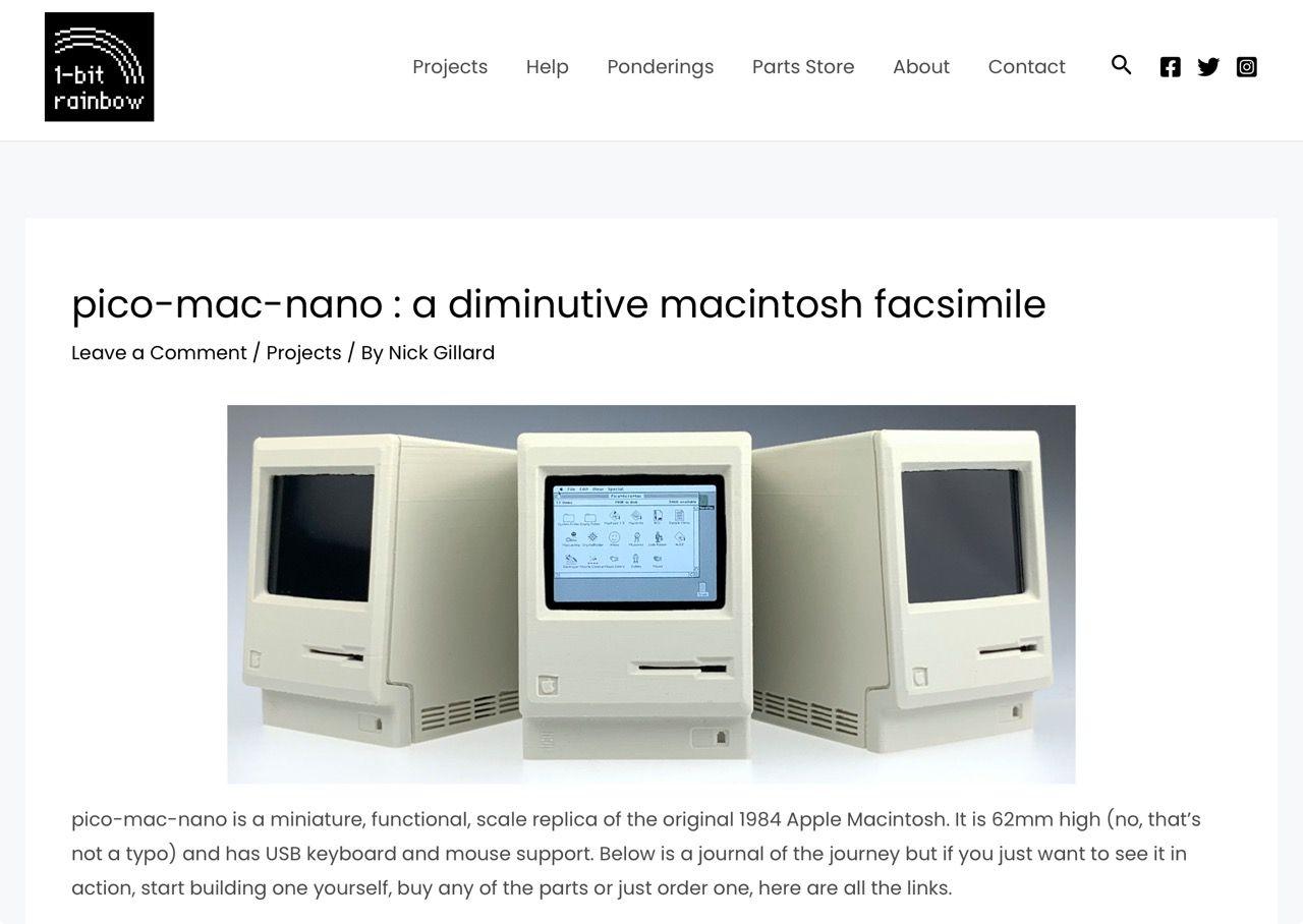
pico-mac-nano: a tiny Macintosh replica
The pico-mac-nano project is the cutest thing I’ve seen in a while, and reminds me of the old SpritesMods ESP32 hack (which I think might still be a bit more functional), but has i(...)
Wtf who designed this shit?
But you've to admit it also is some kind of skill to manage your half height pcie slot cover fitting neatly right in-between four capacitors on the board. (or not, as even though it literally hits the mainboard on one side it still is 0.5cm too long on the other side)...
#pcb #short #perfectfit
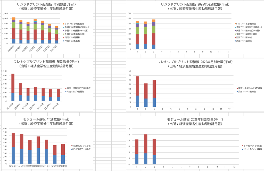
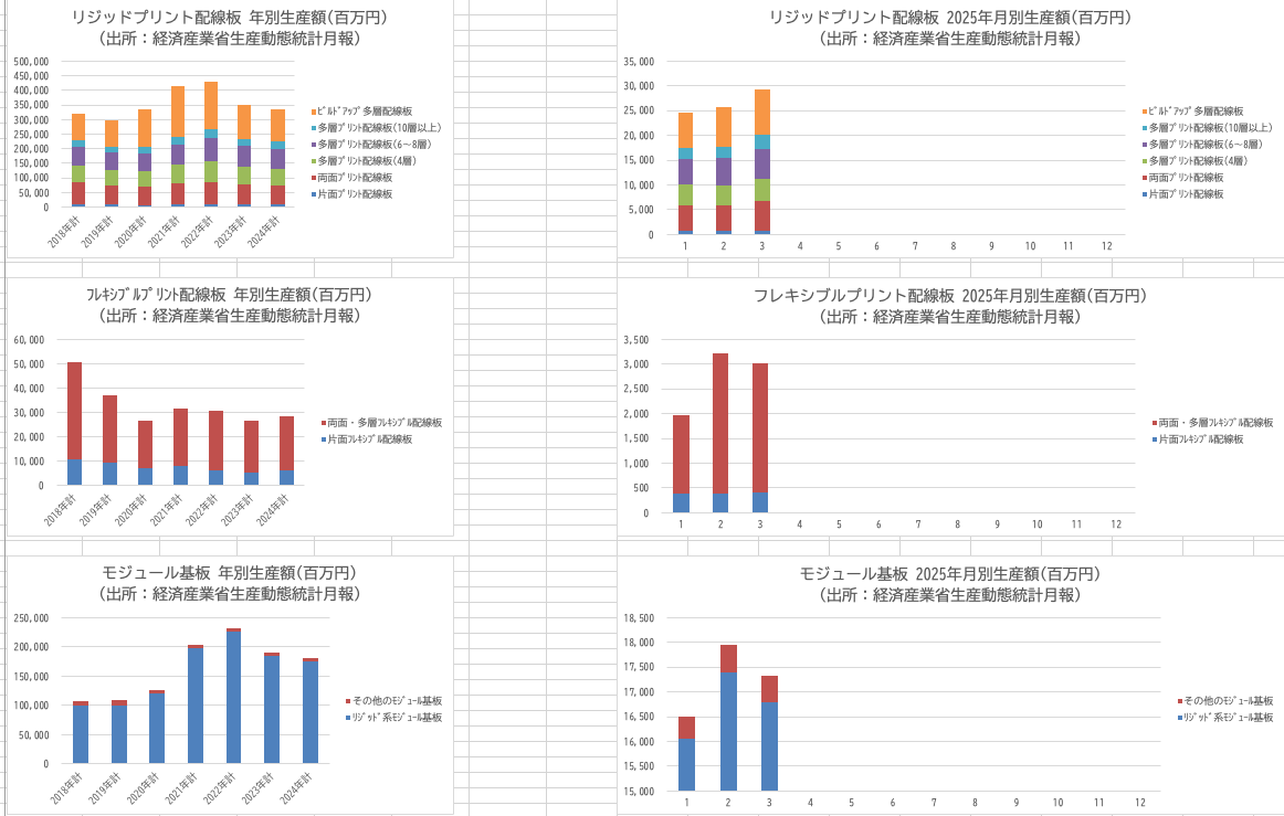
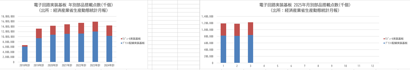
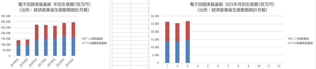
【統計情報】5月23日に日本電子回路工業会 #JPCA が電子回路基板・電子回路実装基板の生産動向資料を更新。2025年3月実績を追加。経済産業省・生産動態統計月報(5月16日公表)による。数量と金額のデータとグラフは https://www.jpcashow.com/kikaitoukei/kikai_toukei.xlsx に(Excel, 190KB)。
#PCB #PCBA #Statistics
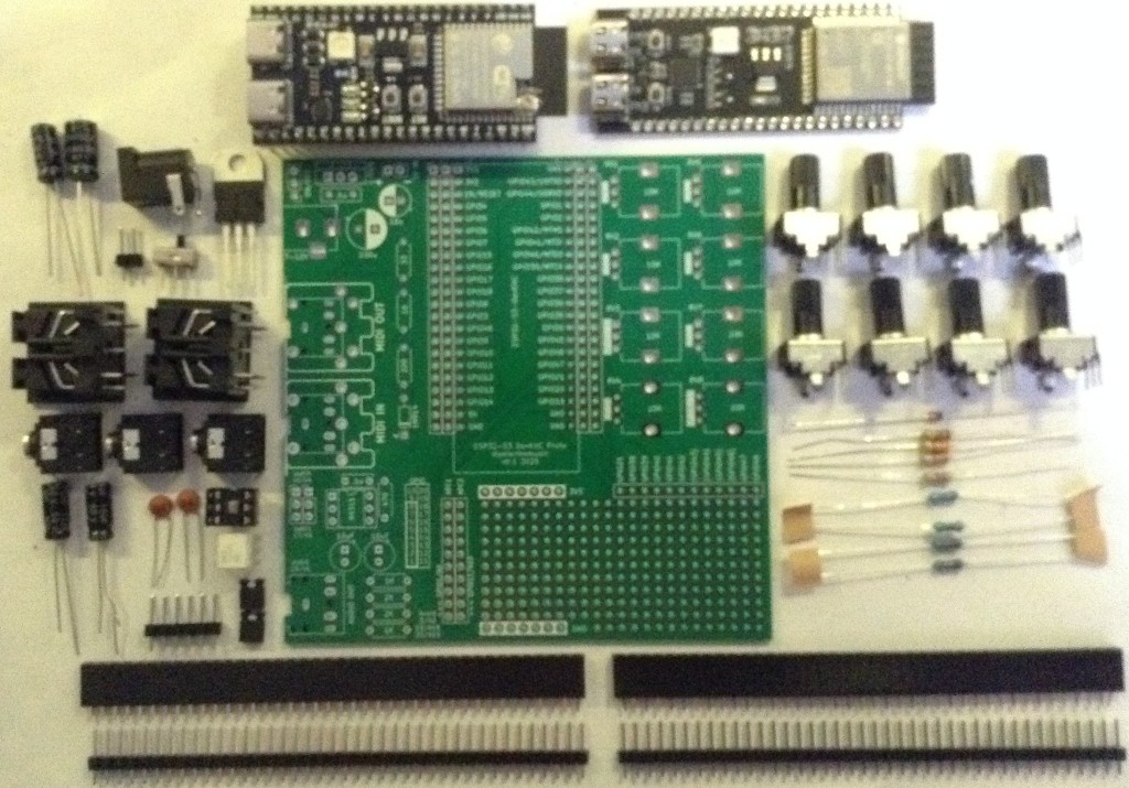
ESP32 S3 DevKit Experimenter PCB Build Guide
Here are the build notes for my ESP32 S3 DevKit Experimenter PCB Design.
Warning! I strongly recommend using old or second hand equipment for your experiments. I am not responsible for any damage to expensive instruments!
If you are new to electronics and microcontrollers, see the Getting Started pages.
Bill of Materials
- ESP32S3 DevKit Experimenter PCB (GitHub link below)
- ESP32S2 DevKitC (official or clone – see ESP32 S3 DevKit)
- MIDI Circuit:
- 1x H11L1 optoisolator
- 1x 1N4148 or 1N914 signal diode
- Resistors: 1x 10Ω, 1x 33Ω, 1x 220Ω, 1×470Ω
- 1x 100nF capacitor
- Either: 2x MIDI DIN sockets (see photos and PCB for footprint)
- Or: 2x 3.5mm stereo TRS sockets (see photos and PCB for footprint)
- Pin headers and jumpers
- Optional: 6-way DIP socket
- Audio Output Circuit:
- Resistors: 2x 1K, 2x 2K
- 2x 10uF non-polar capacitors
- 2x 33nF ceramic capacitors
- 1x 3.5mm stereo TRS socket
- Power Circuit:
- 1x 7805 regulator
- Electrolytic Capacitors: 1x 100uF, 1x 10uF
- 1x 100nF Ceramic Capacitor
- SPST switch with 2.54mm pitch connectors
- 2-way header pins
- 2.1mm barrel jack socket (see photos and PCB for footprint)
- 8x 10K potentiometers (see photos and PCB for footprint)
- Optional: 2x 22-way pin header sockets
- Additional pin headers or sockets as required
Each circuit module is effectively optional. The position of the 22-way headers will depend on which type of module is used. The clone versions are 1 pin row wider than the official version.
There are some solder-bridge configuration options too, which will be discussed later.
Build Steps
Taking a typical “low to high” soldering approach, this is the suggested order of assembly:
- All resistors and diode.
- DIP socket (if used) and TRS socket(s).
- Disc capacitors.
- Switch
- Jumper and pin headers.
- 22-way pin sockets (if used).
- Non-polar and electrolytic capacitors.
- 7805 regulator.
- Potentiometers.
- DIN sockets.
Here are some build photos for the MIDI DIN version of the board. If using MIDI TRS sockets, then these can be installed at the same time as the audio socket.
If using 22-way headers for the DevKit, then the position will depend on which type of DevKit module is being used. In the photo below, I’ve installed 3 sets of 22-way headers to allow me to use either a clone or official module.
The remaining components can almost be installed in any order that makes sense at the time.
Once the main build is complete, two additional capacitors are required for the audio PWM output circuit. Two 33nF capacitors should be soldered across the 1K resistors. This is probably best done on the underside of the PCB as shown below.
Ignore the red patch wire. I managed to cut through a track whilst clipping the excess leads after soldering.
Configuration Options
The following are configurable and can be set by using pin headers and jumpers; solder bridges; or possibly wire links.
- UART for MIDI – pin header + jumpers.
- Audio Output – can be disconnected by breaking solder jumpers on rear of the board under 1K/2K resistors.
- GPIO used for RV3 and RV8 – can be set using solder jumpers on rear of the board under RV3 and RV8.
Testing
I recommend performing the general tests described here: PCBs.
WARNING: The DevKit can be powered from either the USB sockets or the new power circuit, but not both at the same time.
The sample application section includes some simple sketches that can be used to test the functionality of the board.
PCB Errata
There are the following issues with this PCB:
- I should have oriented the DevKit the other way up so that the USB sockets were on the edge of the board, not overhanging the prototyping area!
- The Audio filter requires additional capacitors (see notes).
Enhancements:
- None
Sample Applications
Analog Potentiometers
The following will read all 8 pots and echo the values to the serial monitor.
void setup() {
  Serial.begin(115200);
}
void loop() {
  for (int i=0; i<8; i++) {
    int aval = analogRead(A0+i);
    Serial.print(aval);
    Serial.print("\t");
  }
  Serial.print("\n");
  delay(100);
}
Audio PWM Output
The following will output a 440 Hz sine wave on the PWM channel on GPIO 15. Change to 16 to see the other one.
int pwm_pin = 15;#define NUM_SAMPLES 256uint8_t sinedata[NUM_SAMPLES];#define PWM_RESOLUTION 8#define PWM_FREQUENCY 48000#define TIMER_FREQ 10000000#define TIMER_RATE 305#define FREQ2INC(f) (f*2)uint16_t acc, inc;void ARDUINO_ISR_ATTR timerIsr (void) { acc += inc; ledcWrite (pwm_pin, sinedata[acc >> 8]);}hw_timer_t *timer = NULL;void setup () { ledcSetClockSource(LEDC_AUTO_CLK); for (int i=0; i<NUM_SAMPLES; i++) { sinedata[i] = 127 + (uint8_t) (127.0 * sin (((float)i * 2.0 * 3.14159) / (float)NUM_SAMPLES)); } timer = timerBegin(TIMER_FREQ); timerAttachInterrupt(timer, &timerIsr); timerAlarm(timer, TIMER_RATE, true, 0); ledcAttach(pwm_pin, PWM_FREQUENCY, PWM_RESOLUTION); inc = FREQ2INC(440);}void loop () { }I’m getting a pretty good signal with a 33nF filter capacitor, but the signal still retails some bias. I’m getting a Vpp of around 1.1V.
But it starts out with a swing from around -200mV to +900mV. But this slowly improves over time and after a few minutes is much closer to a nominal -500mV to +600mV. I guess that is probably my cheap capacitors!
MIDI
Most of the MIDI monitors, routers and sending projects I have should work with the MIDI setup. In the default configuration, using UART0 (GPIO 43/44) for MIDI, that appears as Serial0 or the default MIDI configuration (more on serial ports on the ESP32S3 here: ESP32 S3 DevKit).
So the Simple MIDI Serial Monitor should just work and anything sent to the board should:
- Illuminate the on-board (RGB) LED.
- Echo back out to the MIDI OUT port.
Here is the full test code:
#include <MIDI.h>

MIDI_CREATE_DEFAULT_INSTANCE();

void setup() {
  MIDI.begin(MIDI_CHANNEL_OMNI);
  pinMode (LED_BUILTIN, OUTPUT);
}

void loop() {
  if (MIDI.read()) {
    if (MIDI.getType() == midi::NoteOn) {
        digitalWrite (LED_BUILTIN, HIGH);
        delay (100);
        digitalWrite (LED_BUILTIN, LOW);
    }
  }
}
Note: as the MIDI is (probably) hanging of UART0 which is also routed to the USB “COM” port, it will be easier to upload via the USB “USB” port. This won’t clash with the MIDI circuitry on UART0.
Closing Thoughts
I seem to be having a run of “doh” moments with a few of these PCBs, but then that is the price I pay for taking shortcuts by only designing them in my head rather than prototyping them first!
But arguably, it is still a lot easier using a soldered PCB than attempting to build the various elements on solderless breadboard, so in a way that is what these prototypes are largely for.
So apart from the filter issue which is actually fairly easily solved, this seems to work pretty well.
Kevin
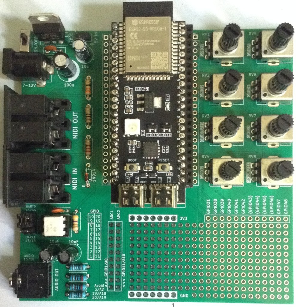
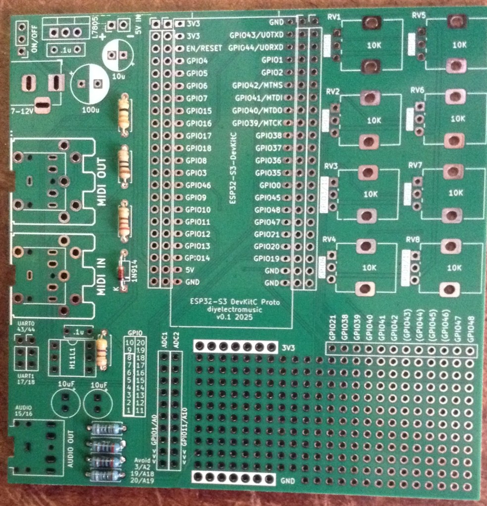
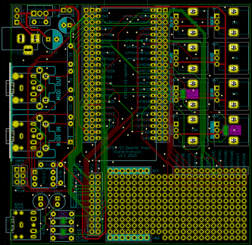
ESP32 S3 DevKit Experimenter PCB Design
This a version of the ESP32 WROOM Mozzi Experimenter PCB for the latest ESP32-S3 DevKitC board I’ve found.
For the background on the boards themselves, see my notes here: ESP32 S3 DevKit.
Warning! I strongly recommend using old or second hand equipment for your experiments. I am not responsible for any damage to expensive instruments!
If you are new to Microcontrollers, see the Getting Started pages.
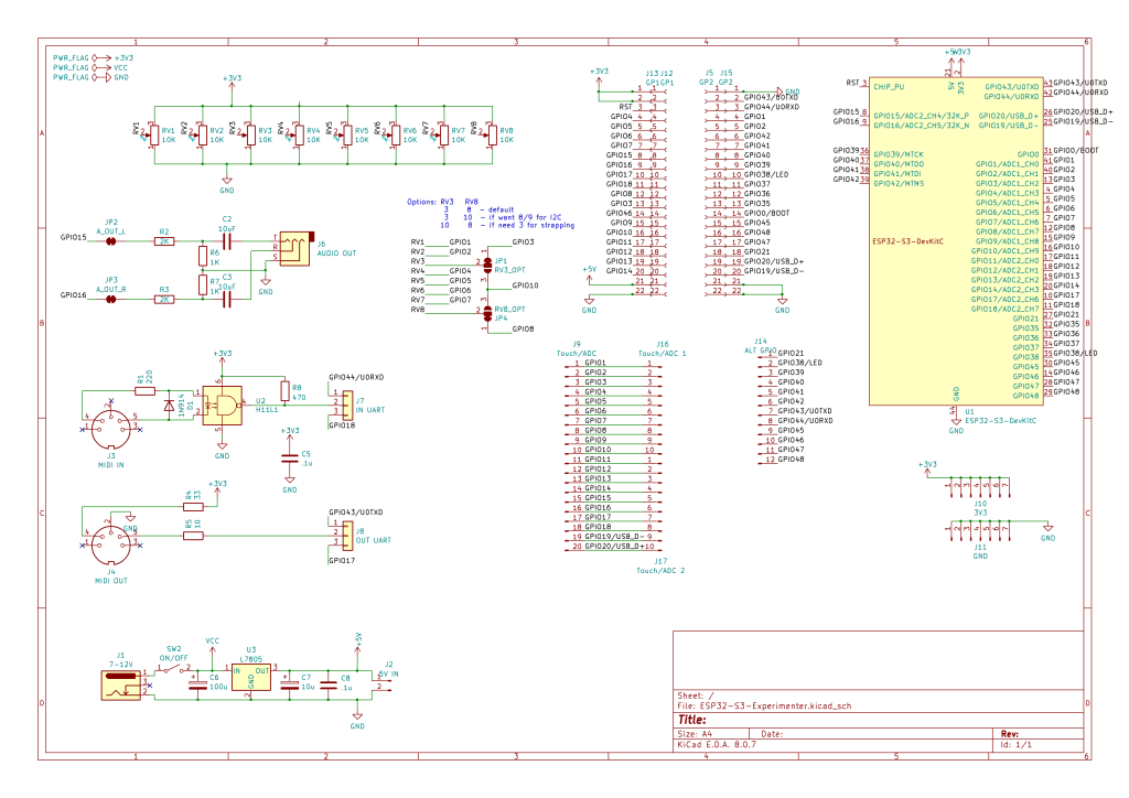
The Circuit
This is mostly just breaking out the pins of the ESP32S3 DevKitC to header pins, but there are a couple of additional features too:
- There are additional rows of headers. The idea is to support the official and clone boards, which means coping with the fact the clone boards are 1 row of pins wider than the official boards.
- There is MIDI IN and OUT with jumpers to select UART0 or UART1.
- There is a stereo PWM output circuit (see notes below).
- There are 8 potentiometers connected to ADC1.
- There is a 7805 or equivalent regulator to provide power if required.
One slight complication is the possibility that GPIO3 (ADC1_CH2) is required as a STRAPPING pin or that GPIO8 (ADC1_CH7) is required for I2C (more in the previous post) so there is a solder bridge option for either of them to switch over to GPIO10 (ADC1_CH9) instead.
The complete GPIO usage is as follows:
GPIO0On board BOOT buttonGPIO 1-8Potentiometer 1-8GPIO 10Optional replacement for GPIO 3 or 8GPIO 15, 16PWM audio outputGPIO 43, 44MIDI if UART0 is selectedGPIO 17, 18MIDI if UART1 is selectedGPIO 1-20Analog breakout area*GPIO 21, 38-49Digital breakout area*GPIO 38 or 48Onboard RGB LED* As already mentioned some of these have alternative or preferred functions.
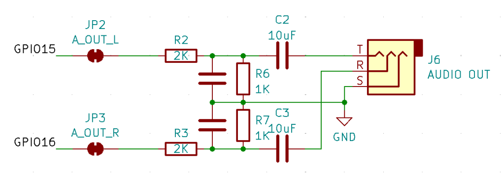
Audio PWM Output
I based this on the output circuit for my ESP32 WROOM Mozzi Experimenter PCB Design, but I was forgetting that the original ESP32 has a DAC and so only requires a potential divider to reduce the voltage levels and a capacitor to remove the DC bias.
The ESP32S3 does not have a DAC, so the output will have to be via PWM if no external DAC is added. This means this output circuit really needs a low-pass filter to smooth out the pulses from the PWM signal.
That hasn’t been included in the design, but can be implemented by adding capacitors across the terminals of the 1K resistors, as shown below.
Following the discussion from Arduino PWM Output Filter Circuit, we can see that a 2K/1K potential divider can (loosely) be treated as a ~666K resistor for the purposes of a low-pass filter calculation. So this gives me various options in terms of capacitor size as follows.
ResistorCapacitorRoll-off frequency666K10nF24 kHz666K33nF7 kHz666K68nF3.5 kHz666K100nF2.4 kHzThe greatest smoothing will come with the lowest cut-off, but 2.4kHz or 3.5kHz will limit the higher audio frequencies somewhat. But a 10nF might not give me enough smoothing.
It will also depend somewhat on the PWM frequency chosen. The higher, i.e. above the audio frequency range required, the better.
I’ll start with adding 33nF and see how that looks then might change with some experimentation.
If an external DAC is used, then there are solder jumpers provided that can be broken to disconnect this part of the circuit anyway.
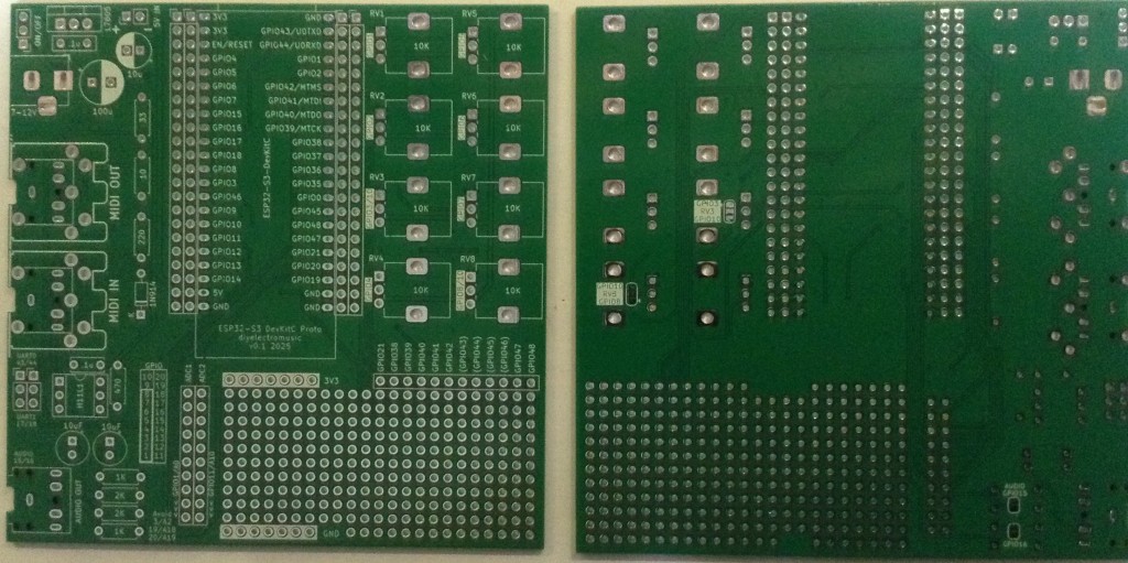
PCB Design
I initially considered only breaking out GPIO pins that weren’t being used for additional functions, but then decided I’d just break them all out alongside the prototyping area. Any pins that might be problematic or have an existing function on the board are labelled in brackets – e.g. (GPIO 43).
The solder jumpers for the GPIO/ADC choices are on the underside of the board.
As previously mentioned, the headers are arranged such that it will support the official DevKitC or the slightly wider clones.
The jumper for UART selection for MIDI can serve as a “disable MIDI to allow use of the serial port” function too if required.
There is also a twin jumper option for direct 5V input instead of going via the barrel jack and regulator.
Closing Thoughts
The omission of the capacitors in the PWM filter is a small annoyance, but it is relatively easily fixed.
Apart from that, there is a fair bit included on this board. It should serve as a good platform for further experimentation.
Kevin

3 hours in, I'm thinking maybe the computer would have been faster, but I didn't feel like screening it today. The pure focal energy of a blank page is unbeatable though.
#handson
#penandpaper
#dotboard
#pcb
#notpcbreally
#design
#electronics
#electrogirl

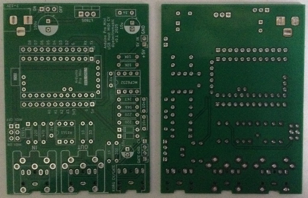
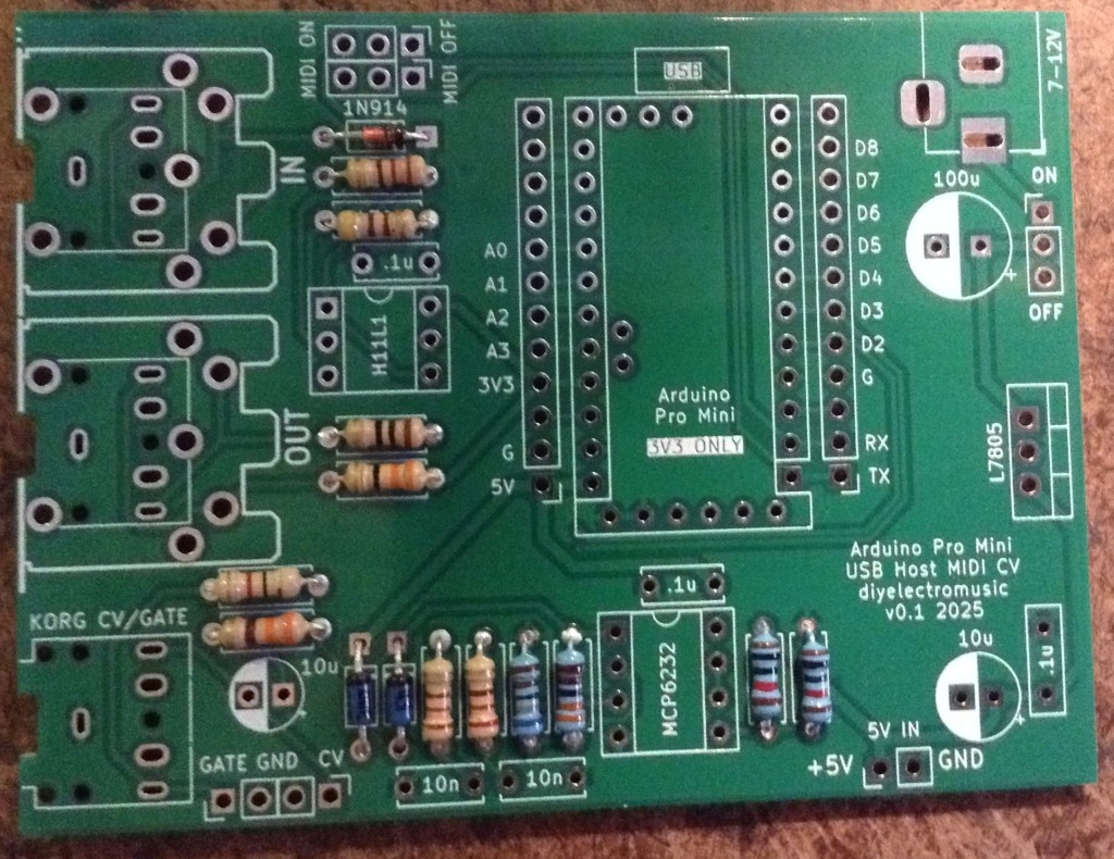
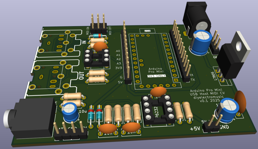
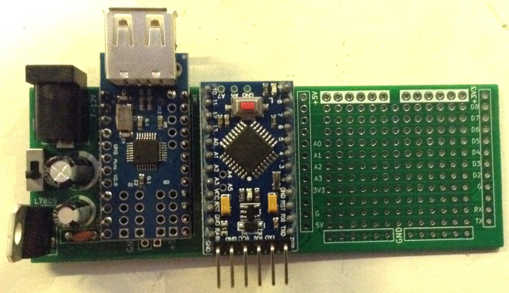
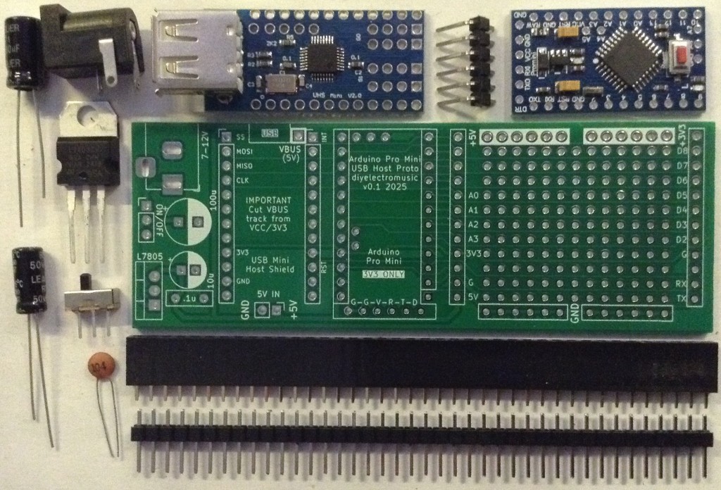
Arduino Pro Mini MIDI USB CV PCB Build Guide
Here are the build notes for my Arduino Pro Mini MIDI USB CV PCB Design.
Warning! I strongly recommend using old or second hand equipment for your experiments. I am not responsible for any damage to expensive instruments!
If you are new to electronics and microcontrollers, see the Getting Started pages.
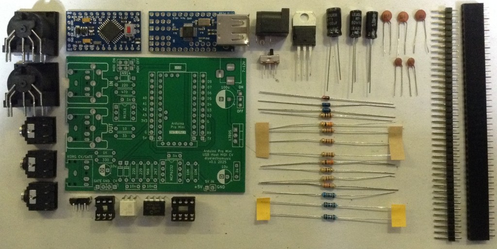
Bill of Materials
- Arduino Pro Mini USB MIDI Host CV PCB (GitHub link below)
- Arduino Pro Mini (3V3/8MHz version)
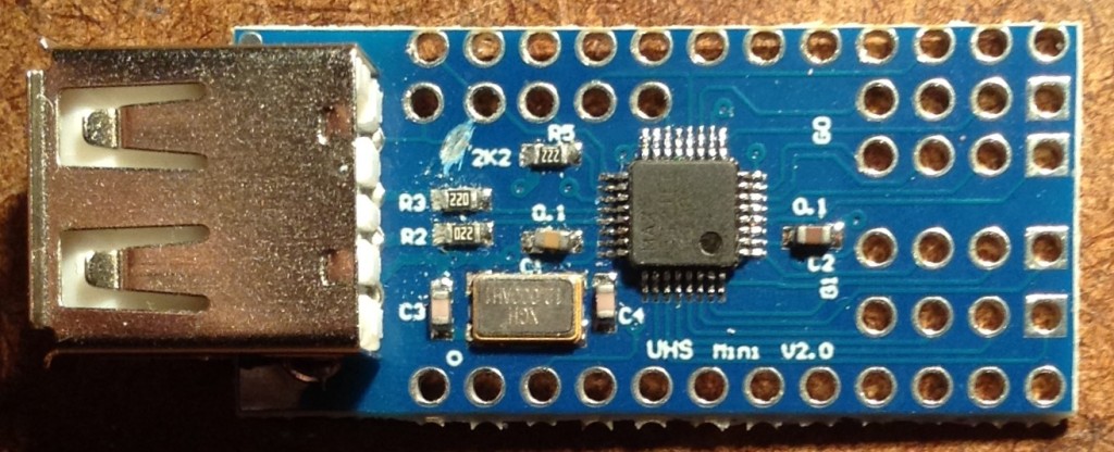
- Mini USB Host Shield 2.0
- 1x H11L1
- 1x MCP6232
- Diodes: 1x 1N4148 or 1N914 signal diode; 2x BAT43 Schottky
- Resistors: 10Ω, 33Ω, 1x 220Ω, 330Ω, 470Ω, 3x 1K, 2K7, 5K6, 2x 10K (*)
- Ceramic Capacitors: 4x 100nF (*)
- 1x 3.5mm stereo TRS
- Either 2x 3.5mm stereo TRS OR 2x 5-pin, 180 degree MIDI DIN sockets
- Pin headers
- Optional: 2x 12-way pin header sockets
- Optional: 1x 6-way DIP socket; 1x 8-way DIP socket
* The PCB shows the use of 2x 10nF and 2x 200Ω resistors for the PWM filter part, but 100nF and 1K work much better.
Optional: Power circuit
- 7805 regulator
- Electrolytic Capacitors: 1x 10uF, 1x100uF
- Ceramic Capacitors: 1x 100nF
- 1x SPST power switch 2.54mm pitch
Build Steps
Taking a typical “low to high” soldering approach, this is the suggested order of assembly:
- Diodes
- Resistors
- DIP sockets (if used) and TRS sockets (if used).
- Disc capacitors.
- Switches (if used).
- Jumper headers.
- Electrolytic capacitors (if used).
- DIN sockets (if used).
- 7805 (if used).
- Arduino + USB Host Shield (see notes below).
The Arduino Pro Mini and USB Host Shield need to be soldered together as a unit. If using header sockets, these will require longer header pins and will need soldering together as a single unit “off board”.
If not using sockets, normal pin-headers should suffice, in which case it is probably easier to solder the pin headers to the PCB and then add the USB Host shield, followed by the Pro Mini.
The USB Host shield requires a track cutting and a connection made from the Arduino’s VIN to the shields VBUS pad. See photos and discussion in the text.
Note: the PCB incorporates a capacitor on the CV PWM output to the TRS socket. This would be required if this was an audio signal to remove the DC bias. But as this is a CV output, the capacitor should be replaced with a simple wire link. More on that below.
Here are some build photos.
The two 220Ω resistors should be replaced with 1K instead.
If using MIDI TRS sockets, these should be added, along with the CV/Gate socket, next with the (optional) DIP sockets.
I’m going to use MIDI DIN sockets, so they will be left almost to last.
The MIDI on/off is required to disabled MIDI to allow sketch uploading to the Pro Mini. This can be replaced with 2×3 pin headers and jumpers, or if the Pro Mini will be removed for programming, even wire links.
I’m using a DPDT slider switch with a 2×3 2.54mm pitch.
The two 10nF capacitors should be replaced with 100nF capacitors instead.
If using 2x 12-way header sockets for the Arduino, these can be added at the same time as other pin headers next.
I’m planning on soldering my USB Host shield and Pro Mini directly to the board, so the best way to do that seems to be to add the headers to the board, as shown below, then I’ll add the shield and Pro Mini later.
The power circuitry is optional. This allows a 7-12V DC barrel jack (centre positive) to be used to create the required 5V for the Pro Mini and USB.
Alternatively, there is a 5V/GND direct jumper header that may be used instead. This should not be used to power the board if the regulator is fitted, but can be used as a 5V source if required.
Note: as already mentioned, when adding the electrolytic capacitors, the 10uF next to the CV TRS socket should be left out and replaced by a wire link.
The full photo below shows the capacitor present – I had to remove it!
The MIDI DIN sockets, if used, are the last component apart from the Arduino itself.
I will be stacking the USB shield and Pro Mini, so the shield goes on next. Note: there is a track that requires cutting between the VBUS solder pad and the 2K2 resistor as shown below. Note, this track must not be cut between the USB socket and the VBUS pad…
Cutting this track removes the connection between the USB VBUS lines and VCC on the PCB, which is running at 3V3. Once cut, a wire can then be soldered between the VBUS pad and the pin that will eventually connect to the Pro Mini’s VIN pin as shown below.
At this point the Pro Mini can now be added on top. I’ve not used any additional spacers, simply relying on the existing solder on the pin headers (from the USB shield) and the presence of the patch wire to distance the board enough. The pin headers themselves weren’t long enough, for me, to add proper plastic spacers, so I didn’t.
Testing
I recommend performing the general tests described here: PCBs.
The sample application section below lists some sketches that will test the various functions of the board.
An oscilloscope can be used to check the voltage output from the PWM signal.
PCB Errata
There are the following issues with this PCB:
- As already mentioned, there are two issues with the CV output circuit:
- The electrolytic capacitor should be replaced with a wire link.
- The 10nF and 220Ω resistors in the filter should be replaced with 100nF and 1K.
Enhancements:
- The CV and GATE signals are different levels at present. CV is 0-5V; GATE is 0-3.3V. Perhaps they ought both be 5V signals.
Sample Applications
The following GPIO pins are used with this PCB:
D0/D1RX/TX for Serial MIDID2GATE outputD3PWM CV outputD9INT pin for USB Host shieldD10-D13SPI link to USB Host shieldHere are some applications to get started with.
Note: I found that serial MIDI would not work when powered via the programming header, presumably because my programmer was controlling RX/TX. To test MIDI the board had to be powered via the barrel jack or 5V directly.
Also recall that MIDI needs to be OFF in order to upload sketches.
- USB MIDI: USB MIDI monitor code here.
- Serial MIDI IN: Simple MIDI monitor code here.
- Serial MIDI OUT: Examples -> USB Host Shield Library 2.0 -> USBH_MIDI -> USB_MIDI_Converter
- GATE Output: Examples -> 02.Digital -> toneMelody (it just produces a square wave)
- PWM Output: Arduino PWM Sound Output (even though this isn’t for sound!)
For the last two, some minor code changes are required.
For toneMelody, the pin used need changing from pin 8 to pin 2 in the tone() and noTone() calls.
For the PWM output, the following configuration options must be set:
//#define FREQPOT A0
//#define PIN_9_PWM_OUTPUT 1   // Uses Timer 1
#define PIN_3_PWM_OUTPUT 1   // Uses Timer 2
In both the GATE and PWM test, it is actually possible to hook up a speaker via a stereo 3.5mm jack to the CV/GATE TRS socket.
WARNING: If you do this, the speaker will be receiving a 0-5V signal on either the L or R outputs (depending on the test). This is a lot more than a line input signal (which is typically +/- 0.8V) so do not hook this up to standard audio input.
Alternatively, just check the signals via the GATE/CV jumper header with an oscilloscope.
The PWM output should be 0-5V. The GATE output should be 0-3.3V.
Use as a USB to CV/GATE Converter
The CV/GATE TRS output follows the standard set for the Korg Volca Modular (see Korg Volca Notes).
I show how to use this as a USB MIDI interface for a CV/GATE synth here: USB MIDI to Serial and CV/GATE.
IMPORTANT: Do not use this board with your Korg Volcas unless you know what you are doing, are able to validate all signals prior to connection yourself, and happy with the very real possibility that the board might do something that damages the Volca.
I am not an electronics person and will not be responsible for damage to expensive or treasured equipment. I only use cheap or disposable equipment in my own projects.
Closing Thoughts
Adding that capacitor was a case of me running on “autopilot” I think, but that is a straightforward fix, so no real harm done.
At the end of the day, this whole board is a little niche, even by my standards.
But it seems to work well enough that I can get on with writing some proper firmware for it now.
Kevin
#arduinoProMini #cv #korg #midi #pcb #pwm #usbHost #usbHostMidi #volca
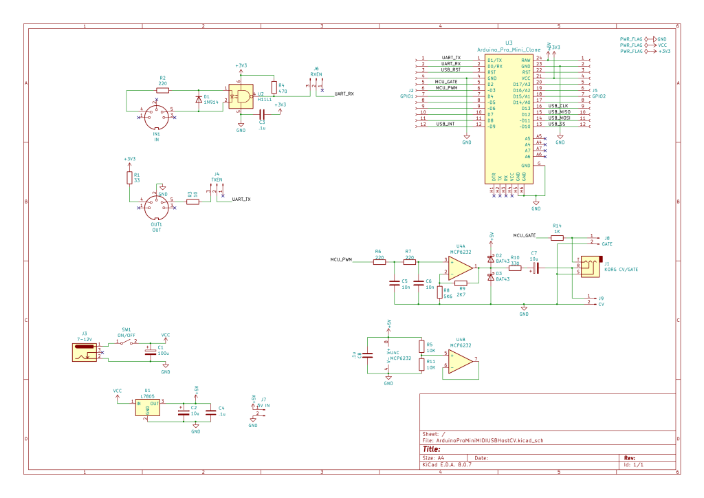
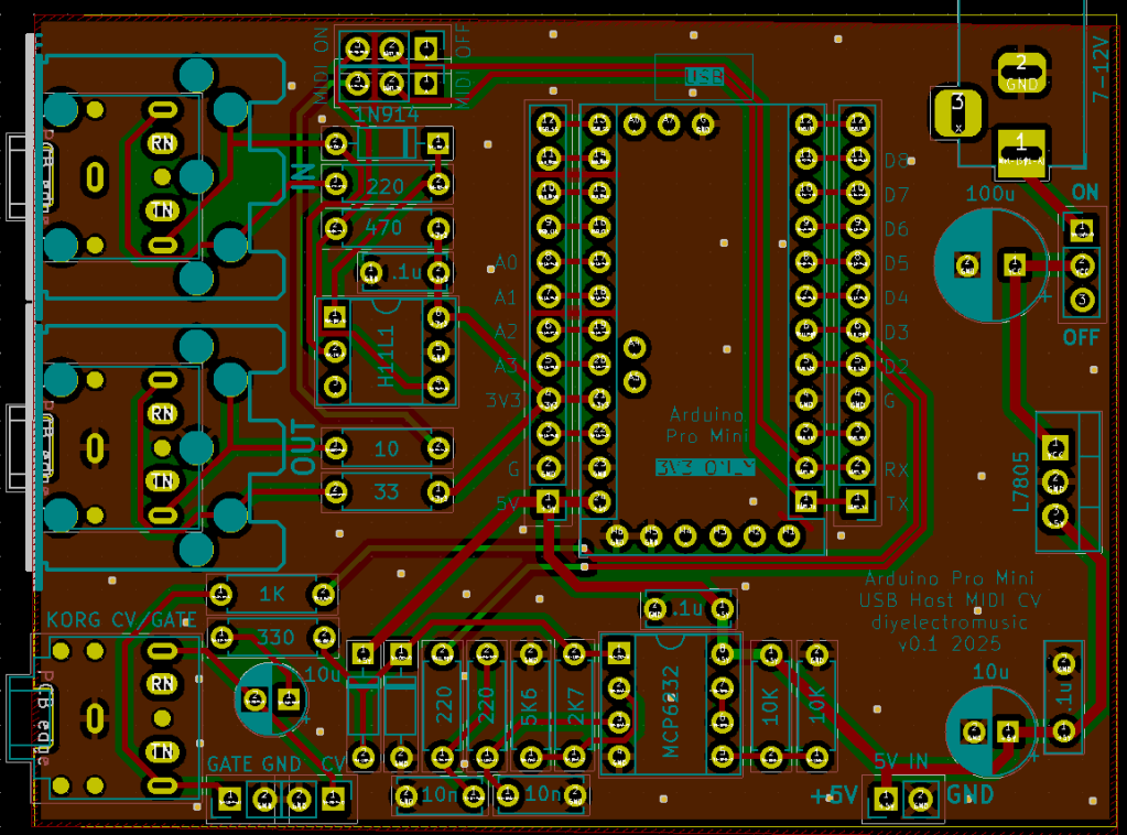
Arduino Pro Mini MIDI USB CV PCB Design
This is essentially a version of my Korg Volca Modular MIDI to CV PCB Design merged with my Arduino Pro Mini MIDI USB HOST PCB Design to give me USB MIDI to serial MIDI and CV.
Warning! I strongly recommend using old or second hand equipment for your experiments. I am not responsible for any damage to expensive instruments!
If you are new to electronics and microcontrollers, see the Getting Started pages.
The Circuit
As previously mentioned this is largely a merging of two existing designs. The main elements are:
- Arduino Pro Mini (3V3/8MHz) with optional USB Host Shield already attached.
- 3V3 compatible Serial MIDI IN/OUT circuit.
- 5V power circuit via a 7805 regulator feeding the VIN of the Pro Mini.
- PWM output filter.
- 3V3 to 5V opamp amplifier stage (largely based on HAGIWO’s designs).
- Korg Volca compatible Gate/CV out via a TRS socket.
I’m using a MCP6232 rail-to-rail dual OpAmp, but I’m only using one of them, so apparently good practice dictates normalising the input of the unused OpAmp to ideally the mid-voltage of the power rails, which I’ve done using two resistors as a potential divider.
The OpAmp is set up for a noninverting amplifier aiming for, as I understand things, a gain of 5/3.3 or ~1.51 as follows:
- Non-Inv Gain = 1 + R(feedback) / R(toground) = 1 + 2K9 / 5K6 = 1.51
Note: the capacitor in the PWM output circuit is actually an error. It isn’t required for a CV output.
Also, the CV output is amplified to make it a 0-5V signal, but the GATE output remains a 0-3.3V signal.
A note on the PWM Filter.
The circuit was originally pasted on from somewhere else and I have to confess I didn’t think about the differing nature of a PWM circuit for a control voltage compared to audio.
As such, the stated component values of 220Ω and 10nF, with a cut-off frequency of upwards of 70kHz whilst useful for audio, are pretty useless for a CV. In the actual build, I’ve used values of 1K and 100nF which gives a cutoff frequency of around 1.5kHz.
That will teach me to properly think about my requirement before cutting and pasting in one of my previous circuits 🙂
PCB Design
Unlike my last design this one assumes the USB host shield will be fixed to the Pro Mini, keeping the footprint as small as possible.
I’ve allowed for both MIDI DIN and TRS sockets. There is also an option for individual GATE and CV out via jumper headers in addition to the Korg Volca compatible TRS.
I’ve included a MIDI switch with the footprint of a 2×3 set of 2.54mm headers so that could be jumpers or a switch as required. If the Pro Mini is socketed (which isn’t so easy if a USB Host shield is attached, but would be possible with longer pin headers), then the MIDI switch could be omitted. It is only there to disconnect MIDI from the Pro Mini UART when uploading sketches.
There is a bit of space around the 7805 in case a small heatsink is required. There is also the option to power the board directly from a 5V supply via a two-pin jumper header.
The Pro Mini footprint includes the programing header, but this isn’t used on the board and should probably be ignored.
Closing Thoughts
My previous MIDI to CV was code for an ATtiny85, so I’ll need to rewrite the code for the ATMega328 on the Pro Mini to support the USB to Serial MIDI routing in addition to CV and GATE.
Kevin

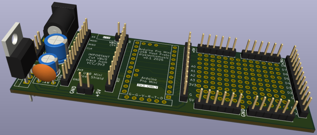
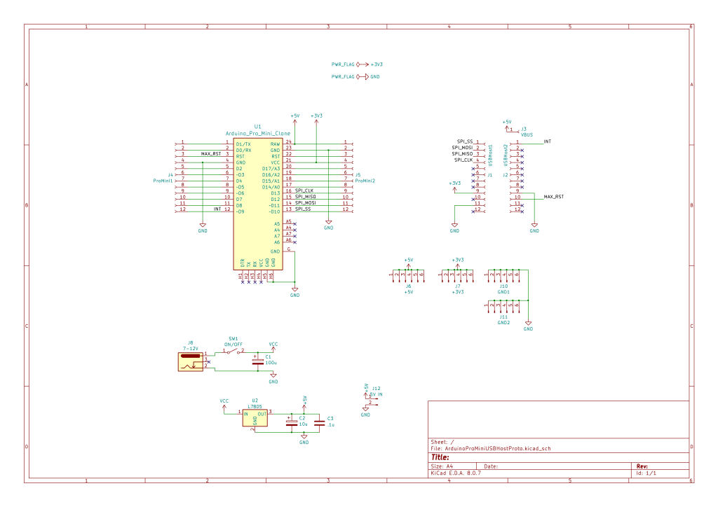
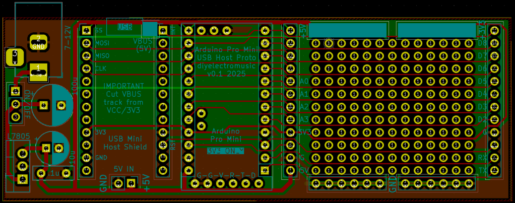
Arduino Pro Mini USB Host Proto PCB Build Guide
Here are the build notes for my Arduino Pro Mini USB Host Proto PCB.
Warning! I strongly recommend using old or second hand equipment for your experiments. I am not responsible for any damage to expensive instruments!
If you are new to electronics and microcontrollers, see the Getting Started pages.
Bill of Materials
- Arduino Pro Mini USB Proto PCB (GitHub link below)
- Arduino Pro Mini (3V3 version)
- Mini USB Host Shield 2.0
- 2x (or 4x) 12-way pin header sockets
- Pin headers
Power supply (optional):
- 1x 7805 regulator
- 1x 2.1mm barrel jack socket (see photos and PCB for footprint)
- 1x 100nF ceramic capacitor
- 1x 10uF electrolytic capacitor
- 1x 100uF electrolytic capacitor
- Optional: 1x slider switch, PCB mount, 2.54mm pitch connectors
The power supply section can be omitted if the board is to be powered directly off 5V, for which an additional 5V/GND set of pin headers is provided.
Build Steps
There isn’t a particular assembly order for this board, but I built it in the following order:
- Prepare the mini USB Host shield (see below).
- Header pins for the mini USB Host shield.
- Header sockets for the Pro Mini.
- Components for the power supply.
The Mini USB Host shield will probably require a track cutting to isolate VBUS from the 3V3 supply of the Pro Mini. The track in question links the VBUS solder pad to the nearby 2K2 resistor. The track needs to be cut between the pad and the resistor, but care is needed to ensure it isn’t cut on the “USB” side. See photo below.
Here are some build photos.
Notice in the above there is an additional single pin for the VBUS connection. I’ve used pin headers rather than a socket to allow me to mount the USB Host shield permanently on the board.
If a socket is used then it will be necessary to find an alternative means to connect the VBUS pad on the shield to the VBUS or 5V connection on the PCB.
I’m not using any headers for the Pro Mini’s programming connection. This doesn’t actually do anything on the PCB and is really just there for helping to orient the board.
In the following, I’ve only actually soldered the pins on the USB Host shield that are used to connect it to the Pro Mini. There are 9 in total, not including VBUS, and all, apart from a second GND, are labelled on the PCB:
- Top four pins on the left (SS, MOSI, MISO, CLK).
- Topmost single pin on the right (IN).
- GND and 3V3 on the left (2nd and 4th from the bottom).
- GND and RST on the right (3rd and 4th from the bottom).
If used, I soldered the power supply components last.
Testing
I recommend performing the general tests described here: PCBs.
Note: when programming the Pro Mini an additional programming header is required.
Some of the cheap programmers do not accurately set the voltage for powering the board, even if there is a switch for 5V/3V3 operation, so it is worth double checking prior to use.
If an external 5V connection is required, the additional GND/5V header pin at the bottom of the USB Host shield can be used.
PCB Errata
There are the following issues with this PCB:
- None at this time.
Enhancements:
- I’ve included a footprint for the programming header, but it doesn’t do anything or go anywhere.
Sample Applications
Here is a simple USB MIDI monitor application that can be used to see if the board is working:
Closing Thoughts
As I say, I’m not sure this will get a lot of use, but it can go in the bits box for a rainy day!
Kevin

Arduino Pro Mini USB Host Proto PCB Design
This is a prototyping board for an Arduino Pro Mini and mini USB Host shield.
Warning! I strongly recommend using old or second hand equipment for your experiments. I am not responsible for any damage to expensive instruments!
If you are new to electronics and microcontrollers, see the Getting Started pages.
The Circuit
This is mostly just breaking out the pins for an Arduino Pro Mini onto a set of additional headers for use with a mini USB Host shield.
There are additional headers for power and GND and it includes the option for powering via a 7-12V barrel jack into via a 7805 regulator or directly via 5V into a set of jumper header pins.
PCB Design
In previous designs I’ve opted to assume that the USB host shield will be mounted directly onto the Arduino Pro Mini, but this time I’ve separated them out for more flexibility.
I may decide I should have just left them together, but I didn’t think I’d be able to use pin headers and sockets in quite the same way with the headers already connecting two boards.
With hindsight I’m now wondering if I should have passed through all the Arduino Pins to the shield part. As it stands, it only has the connections required for the USB host shield.
All of the pins are broken out either side of the prototyping area however, but only the usable pins have been labelled.
Closing Thoughts
This was a somewhat speculative build based on the idea that I’d want to experiment with a USB host device and some additional circuitry.
But my main need has been satisfied by an alternative build (more on that later), so for now this is probably a “why not, might come in useful” build.
Kevin
My Two Cents on Pakistan T20 Squad vs Bangladesh
#thedarkknaik #pakistan #pakistancricketteam #pakvban #pakistanvsbangladesh #sufiyanmuqeem #abbasafridi #faheemashraf #babarazam #mohammadrizwan #shaheenafridi #shahidafridi #imrankhan #indiavspakistan #sahibzadafarhan #hassannawaz #psl #lahore #pcb #bangladesh #bangladeshcricket
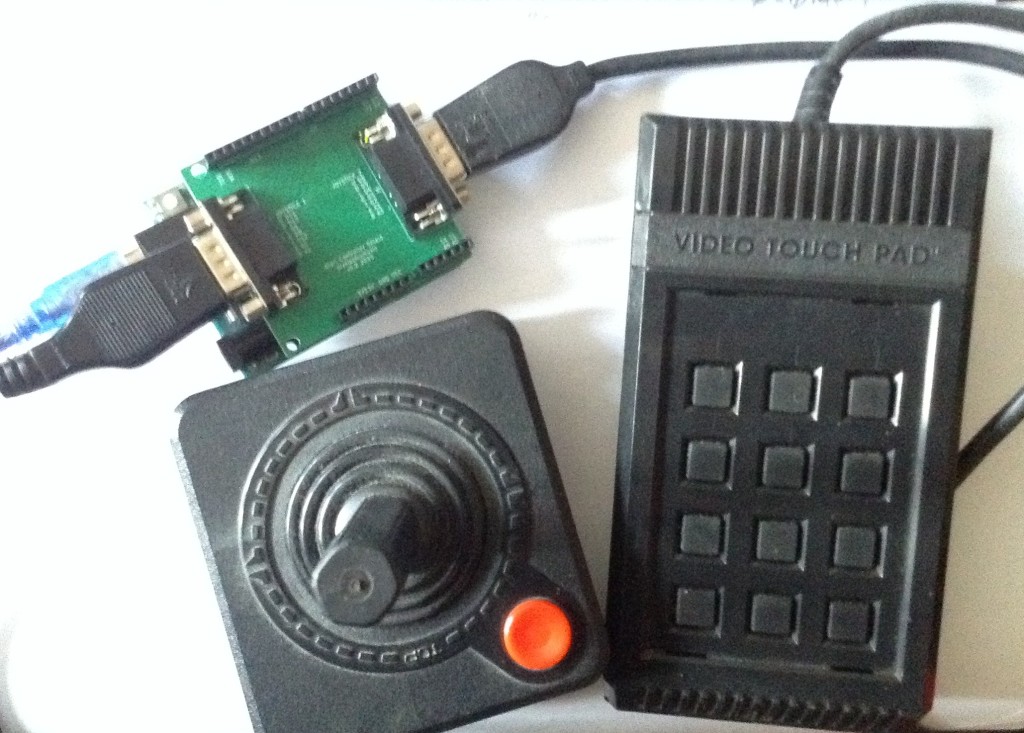
Atari 2600 Controller Shield PCB Build Guide
Here are the build notes for my Atari 2600 Controller Shield PCB Design.
Recall from my design notes that this version doesn’t deal with paddles very well.
Warning! I strongly recommend using old or second hand equipment for your experiments. I am not responsible for any damage to expensive instruments!
If you are new to Arduino, see the Getting Started pages.
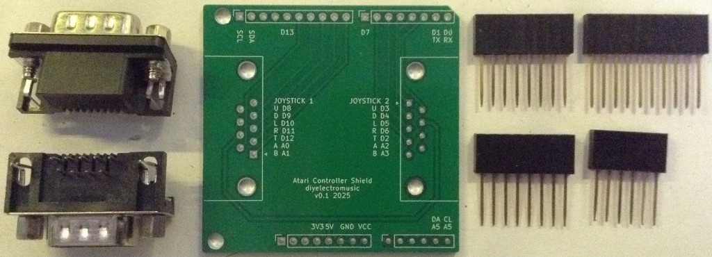
Bill of Materials
- PCB (GitHub link below)
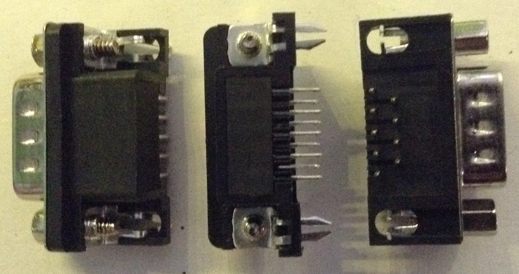
- 2x 9-pin D-type connectors – PCB mounted (see photos and PCB for footprint).
- Optional: Arduino headers: 1×6-way, 2×8-way, 1×10-way
- Or: pin headers
The above photo shows the 9-pin D-type connectors from various angles. The spacings are as follows:
- Pin spacing: 2.77mm
- Spacing between pin rows: 2.84mm
- Distance from pins to edge of connector: 7.7mm
- Mounting hole distance to edge of connector: 9.12mm
- Mounting hole distance: 25.0mm
Build Steps
It doesn’t matter much whether the pin headers or D-type connectors are soldered first.
However, if using header sockets as shown in the photo above, then it makes more sense to fix these first as they need to be soldered on the same side as the D-types, but aren’t as tall.
Testing
I recommend performing the general tests described here: PCBs.
A simple digital and analog read sketch can be used to quickly check the functionality.
For joysticks:
#define PINS 10
int p[PINS] = {2,3,4,5,6,8,9,10,11,12};

void setup() {
  for (int i=0; i<PINS; i++) {
    pinMode (p[i], INPUT_PULLUP);
  }
  Serial.begin(9600);
}

void loop() {
  for (int i=0; i<PINS; i++) {
    Serial.print(digitalRead(p[i]));
    Serial.print("\t");
  }
  Serial.print("\n");
  delay(200);
}
For paddles:
Note: this will require an additional resistor to GND from the corresponding analog input, for all paddles used. If a 1M resistor is used there is a more linear response, but the readings will only vary between 512 and 1023 (or thereabouts) corresponding to a read voltage of between 2.5V and 5V.
void setup() {
  Serial.begin(9600);
}

void loop() {
  for (int i=0; i<4; i++) {
    int aval = analogRead(A0+i);

    Serial.print(aval);
    Serial.print("\t");
  }
  Serial.print("\n");
  delay(100);
}
For keypads:
Note: this requires the keypad library which should be available by default with the Arduino environment.
#include <Keypad.h>

const byte ROWS = 4; //four rows
const byte COLS = 3; //three columns
char hexaKeys[ROWS][COLS] = {
  {'3','2','1'},
  {'6','5','4'},
  {'9','8','7'},
  {'#','0','*'}
};
// Port 1
byte rowPins[ROWS] = {11,10,9,8};
byte colPins[COLS] = {12,A0,A1};
// Port 2
//byte rowPins[ROWS] = {6,5,4,3};
//byte colPins[COLS] = {2,A2,A3};

Keypad customKeypad = Keypad( makeKeymap(hexaKeys), rowPins, colPins, ROWS, COLS);

void setup(){
  Serial.begin(9600);
}

void loop(){
  char customKey = customKeypad.getKey();

  if (customKey){
    Serial.println(customKey);
  }
}
PCB Errata
There are the following issues with this PCB:
- As already mentioned there is no real provision for reading paddles.
Enhancements:
- Allow for a resistor and capacitor to mirror the original Atari 2600 circuit.
Closing Thoughts
As is becoming customary, it appears I can’t produce a PCB without at least one annoying issue. Even one as simple as this I managed to get the wrong sense for the connector for v0.1 and didn’t notice until the signals weren’t working!
The paddle issue was really just my misunderstanding (misreading) of the documented paddle circuit!
But pleasingly the Arduino built-in Keypad library “just works” with the keypad controllers and this simple version of the Arduino shield
Kevin
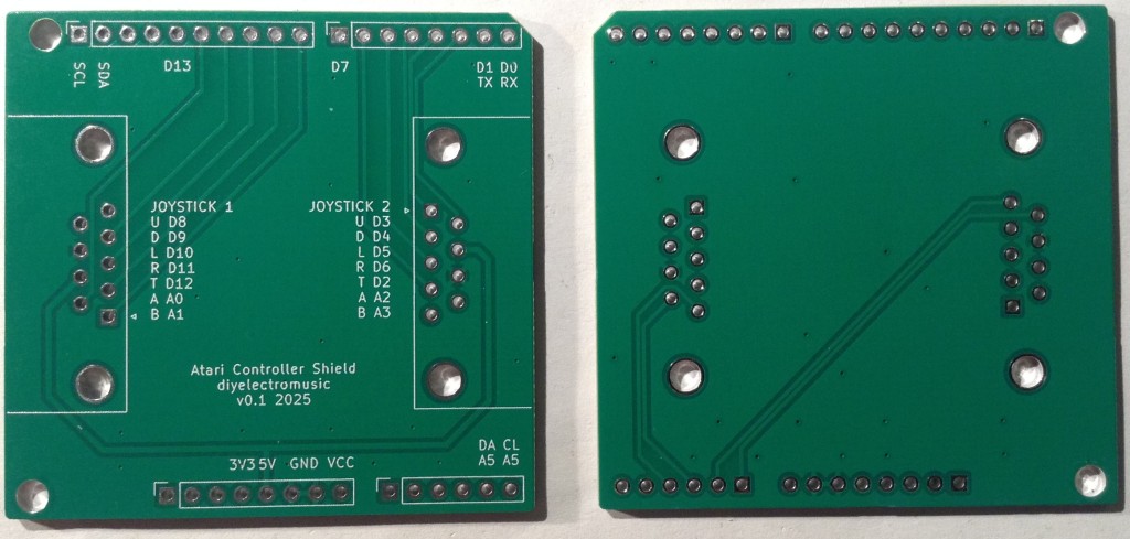
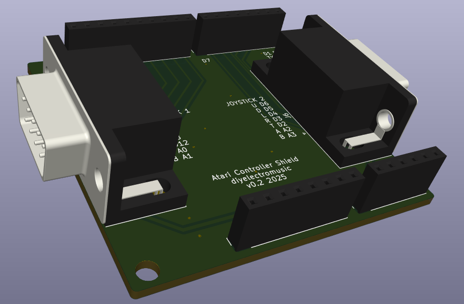
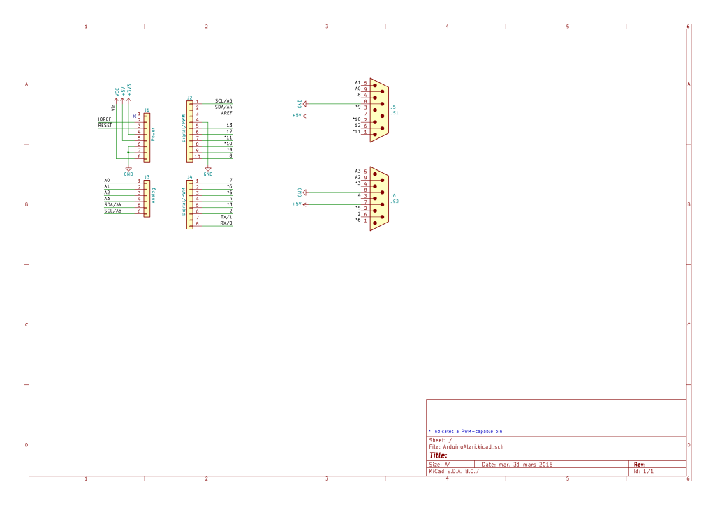
Atari 2600 Controller Shield PCB Design
This is an Arduino Uno shield format PCB for hooking up two Atari 2600 style controllers to an Arduino.
Note: this iteration of the design doesn’t really do the paddles very well, but it works fine for joysticks and keypad controllers.
Warning! I strongly recommend using old or second hand equipment for your experiments. I am not responsible for any damage to expensive instruments!
If you are new to Arduino, see the Getting Started pages.
The Circuit
This is a fairly straight-forward mapping of an Atari controller’s pins to Arduino IO pins.
The most comprehensive description I’ve found of what the 9 pins on the D-type connector are is the following. And there are a few other useful references too:
- https://atariage.com/2600/archives/schematics/Schematic_2600_Accessories_Low.html
- https://forums.atariage.com/topic/225470-the-atari-joystick-pinout-common-ground/
- https://www.epanorama.net/documents/joystick/ataristick.html
On driving them with an Arduino, the following are relevant:
- https://hackaday.io/project/170908-control-freak
- https://github.com/nomdeclume/AtariJoysticksPlus
- https://github.com/retrospy/RetroSpy
Standard Joysticks
The buttons are pulled high, connected low when the button is pressed. This makes reading the joystick and paddle buttons relatively straight forward.
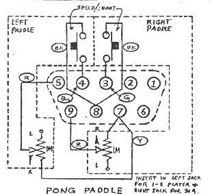
Paddles
The analog paddle inputs are a little more complicated. On first inspection, I thought they were effectively potentiometers across 5V and GND, but actually it turns out they are 1M variable resistors across 5V and the wiper. This means that reading them is a little more complex.
To read them using a simple ADC method, it is possible to include a second resistor between the controller pin and GND, creating a voltage divider that can then be read via the ADC. The smaller the second resistor, the more of the voltage range will be covered.
But it isn’t a typical voltage divider. As R1 changes, the percentage of R2 changes too, so whilst a small R2 gives more of the voltage range (closer to 0V up to 5V), the change is less linear.
Here are some graphs showing the output voltage profile for different R2 values.
So 1M (which of course matches the resistance already in the paddle controller pot) gives the most linear response, but it has the following properties:
- Read value = 0V -> controllers not present.
- Read value between 2.5V and 5V -> controller present and being used.
The actual Atari circuit appears to have a 1.8K resistor into the microcontroller pin with a 68nF capacitor to GND (follow the circuit from pins 5 and 9 here). From some of the above links for using paddles with an Arduino it appears the basic algorithm for reading the paddles is to time the charging and discharging of the capacitor.
There is no facility on this version of the board to allow for the addition of a capacitor and a resistor. It is possible to include a resistor to GND in some cases, but really the use of this board with paddles is quite sub-optimal!
Keypads
When used with a keypad, the four direction buttons are mapped to rows, and the two paddle inputs (pulled up in the controller to 5V) and trigger is used for the columns.
Arduino GPIO
From all this, we can derive the following table and map that over to Arduino IO pins. I’ve added two 9-pin connectors, so they are mapping onto two sets of Arduino pins.
Atari PinJoyStickPaddlesKeypadArduino port 1Arduino port 21UPROW11162DOWNROW21053LEFTTRIGGER AROW3944RIGHTTRIGGER BROW4835PADDLE BCOL1A1A36TRIGGERCOL312275V5V5V8GNDGNDGND9PADDLE ACOL2A0A2As A0-A3 can be used as either digital or analog inputs this makes decoding the controllers particularly easy (paddles not withstanding) once it is known what kind of controller is attached.
PCB Design
The PCB design is quiet straight forward. The IO pins have been chosen for easy routing. I’ve used footprints for the two controller connectors that matched the PCB-mount connectors I’ve been able to pick up fairly cheaply.
All unused Arduino IO pins have been labelled on the board for ease of use. The following are all available:
- D0/D1 – RX/TX
- D7, D13
- A4, A5 – SDA/SCL
This leaves options for UART, I2C, digital and analog IO.
As already mentioned, no provision has been included for sensible decoding of the paddles. That will have to come in a future version.
Closing Thoughts
In the first iteration of this board, although it is a pretty straight forward board, I’d managed to use the footprints for the socket version of the 9-pin connectors and not the pins version.
This meant that when I got the boards back, the pins were all back to front!
I had a quick re-spin of the board, including swapping the pins associated with UDLR over so that routing remained fairly trivial.
If I’d looked at the 3D version of the board prior to sending it off, I might have noticed. Oh well.
The whole thing with the paddles was because I’d mis-read the schematic for the controllers and made the assumption that they were wired between 5V and GND in a common potential divider format.
It wasn’t until the boards came back and the paddles weren’t working that I looked a bit deeper and spotted the misunderstanding. Oh well.
Kevin

Da @PCBWay una nuova apparecchiatura di stampa UV in grado di stampare #PCB a colori, mediante l'uso di inchiostri a polimerizzazione UV per ottenere immagini di alta qualità su vari materiali, tra cui schede in fibra di vetro, substrati metallici, substrati ceramici, schede flessibili e schede rigide-flesse.
Leggi la notizia completa 👉🏻PCBWay https://www.elettronica-tech.it/stampare-pcb-a-colori/?utm_source=mastodon&utm_medium=Zoho+Social e registrati su #ElettronicaTECH per non perdere tutti gli aggiornamenti!
Bin noch immer ein Fan der Idee #brushless-#Motoren als #PCB zu fertigen - https://microbots.io/products/motorcell
Wenn man die noch als Stepper-#Motor ausbauen würde, wäre das das ultimative Bauteil für wirklich winzige/integrierte Aktuatoren.
Leider ist wohl "kauf einfach einen billigen Motor und mach paar Drähte ran" immer billiger als sowas in's eigene PCB zu integrieren und den Motor selbst zusammenzubauen.
Und ich hab ja auch noch so 0703-Motoren (7mm Durchmesser, 3mm Stator-Höhe) die fertig geliefert werden und ebenfalls unfassbar kompakt sind. (idk was gewicht/leistung besser tut)
ESP32 S3 DevKit
Having played a bit with ESP32-S3 now, in the of the Waveshare Zero format boards, I’d quite like to have a version of the ESP32 WROOM Mozzi Experimenter PCB for the latest ESP32-S3 DevKitC board I’ve found.
This is the introductory post that is my “notes to self” as I get to know the boards.
Warning! I strongly recommend using old or second hand equipment for your experiments. I am not responsible for any damage to expensive instruments!
If you are new to Microcontrollers, see the Getting Started pages.
ESP32-S3 DevKitC Boards
There are a couple of ESP32-S3 official DevKits, in addition to the huge range of third party boards from the likes of Waveshare, Adafruit, and so on of course.
The main references for these boards are:
- ESP32-S3 SOC page
- ESP32-S3 datasheet
- ESP32-S3 WROOM-1/1U/2 modules
- ESP32-S3 DevKitC-1 – based on the WROOM modules
- ESP32-S3 DevKitM-1 – based on the Mini modules
Note: although the C and M DevKits both have 44 pins and very similar functionality, the actual pinouts for the two boards are quite different. On the face of things, it looks like the pinout for the M version seems a bit more logical to me than the C version, but I’ve ended up with C boards, so that is what I’m going with! Much of what follows is applicable to both though.
It is also worth noting that I was looking at the ESP32-S3 as a possible replacement for the original ESP32 in my Educational DIY Synth Thing. But in terms of general features, the ESP32-S3 and ESP32 are actually pretty similar.
From the comparison here, here are some key features listed:
ESP32ESP32-S332-bit LX632-bit LX7single or dual coredual core240MHz (one variant at 160MHz)240MHz520KB SRAM512 KB SRAM448 KB ROM384 KB ROM0MB, 2MB, 4MB Internal Flash0MB, 8MB Internal FlashUp to 16MB External FlashUp to 1GB External FlashUp to 8MB External RAMUp to 1GB External RAMMost of the peripherals are pretty similar too.
So the key difference is the switch from LX6 to LX7. As both support a single-precision floating point unit, and up to 240MHz operation in dual core modes, I’m not sure what the enhancement is at the moment.
One difference on Wikipedia is that the LX7 has “added instructions to accelerate machine learning applications” and it appears that there is a specific library that makes use of these instructions: ESP-DL. But I’ve not seen if any of this is likely to help me with audio.
I should also note that the original ESP32 is the only chip in the architectural family (as far as I can see) with an integrated DAC. There is certainly no DAC with the ESP32-S3.
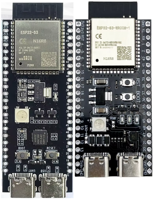
I was determined to go with the official ESP32-S3 DevKitC board this time. But on my first attempt I managed to end up with a very close clone! I have now have two variants as shown below. The original is on the left and the clone on the right.
The clones are very similar to the original but seem to have the following differences.
Physical Differences:
- The clone is shorter and 2.54mm (i.e. a “pin row”) wider.
- Buttons are in a different place.
- USB-C ports in different place compared to the GPIO pins.
Electrical Differences:
- The USB ports are swapped. The original has UART on the left, USB on the right. The clone is swapped.
- Clone has a solder jumper on the rear for USB-OTG for the USB port. If soldered, this shorts a diode in the VBUS 5V line to allow the USB port to power an external device.
- Original has an SK68xx LED (powered from 3V3), the clone has a WS2812 (powered from 5V), although they should be essentially the same code/protocol wise.
- Original has the LED on GPIO38 (maybe – mine doesn’t). Clone has LED on GPIO48.
- Clone has a solder jumper for the LED which is connected by default.
- Original uses a CP2102N USB serial chip. Clone has a CH343P.
- Original uses a SGM2212 regulator which has a 2.7-20V input range. Clone uses a CJ6107 with range 2.5-6V. Although in both cases the input is essentially 5V from USB VBUS.
- The clone has an IN-OUT solder jumper. If soldered, this shorts a diode on header pin 21 (5V) to allow power to be fed into the board via the 5V pin.
- The clone has a RX and TX LED.
- The clone has the (strapping) pin 3 pulled HIGH to 3V with an additional 0R resistor in place in case that is not required.
Documentation for the original board: https://docs.espressif.com/projects/esp-dev-kits/en/latest/esp32s3/esp32-s3-devkitc-1/user_guide.html
Documentation for the clone: https://github.com/vcc-gnd/YD-ESP32-S3/tree/main/5-public-YD-ESP32-S3-Hardware%20info
At least the pinouts for the two modules seem the same, apart from the fact that one module is one-pin-header-row wider than the other.
ESP32-S3 DevKitC-1 GPIO Use
Strapping pins are used to set the configuration of the ESP32-S3 on power up. For details of the strapping pins and their use, see Section 4 in the ESP32-S3-WROOM-1 guide. The summary, and default settings for the ESP32-S3, is as follows:
GPIO0BOOT modeWeak pull-up to 1SPI bootGPIO3JTAG signal sourceFloatingEFUSE_STRAP_JTAG_SEL=0; GPIO3 ignored.EFUSE_STRAP_JTAG_SEL=1; GPIO3=1 USB; GPIO3=0 JTAG pins.GPIO45VDD_SPI voltageWeak pull-down to 0GPIO46ROM message printingWeak pull-down to 0
Working through the datasheets, schematics and online guides, as far as I can make out the following GPIO pins all have an expected use on the DevKitC-1 boards, which can limit their use for general projects.
GPIOUse0, 3, 45, 46ESP32-S3 Strapping pins as described above.15, 16Optional: can be used to connect an external oscillator – not used on these boards.19, 20USB OTG port data connection35, 36, 37Onboard SPI flash memory43, 44UART0 connection to USB serial chip47, 48If a N16R16VA module (16MB Flash, 16MB PSRAM) is used then these pins operate at 1.8V.38 or 48WS2812 compatible RGB LEDTaking account of all the above, this leaves the following GPIO pins probably available for use in projects:
GPIO Range#PinsNotes1-22GPIO, Touch, ADC4-1613GPIO, Touch, ADC17-182GPIO, Touch, ADC, UART119-202GPIO, USB, ADC211GPIO381GPIO, LED on official board39-424GPIO, JTAG43-442GPIO, UART0471GPIO*481GPIO*, LED on clone board (can be disabled)So this would hopefully give me access to 19 GPIO that could act as analog inputs and a further 7 GPIO in addition to two for RX/TX.
This assumes that GPIO 47 and 48 not operating with an SPI flash configuration that means they will run at 1.8V. For the modules I have I’m using a ESP32-S3-N16R8 module so this should be fine as this only applies to the N16R16VA variants of the modules.
In terms of functions, the way the ESP32-S3 supports GPIO multiplexing means that any of these could be configured for I2C or I2S, and they all support PWM outputs.
For a more detailed discussion of the restrictions, see https://github.com/atomic14/esp32-s3-pinouts
EPS32-S3 and Arduino
Serial Ports
There are several options for serial ports:
- Native USB (the “USB” USB port)
- USB via UART0 (the “COM” USB port)
- UART0 directly via TX/RX
- UART1 via GPIO
These map onto the following serial options in Arduino (see cores/esp32/HardwareSerial.h):
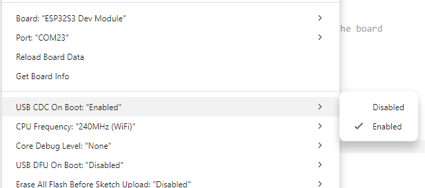
DeviceArduino DeviceArduino aliasNative USBUSBSerialSerial (if ARDUINO_USB_CDC_ON_BOOT set)USB via UART0Serial0Serial (if ARDUINO_USB_CDC_ON_BOOT not set)UART0Serial0UART1Serial1There is a build option that determines whether the loaded code includes a USB comms device or not.
If this isn’t set (i.e. “disabled”) then Serial goes to UART0 and the serial monitor has to be connected to the “COM” USB port.
If this is set (i.e. “enabled”) then Serial goes to USBSerial and the serial monitor can be connected to the “USB” USB port.
Note: there is some ESP32 start-up debug information that will always go to UART0 on boot regardless of this setting.
Analog Input
One quirk of the ESP32 Arduino environment and the ADC mapping means that the ADCs are mapped as follows:
- ESP32 ADC1 peripheral: channels 0 to 9 = GPIO 1 to GPIO 10 = Arduino A0 to A9
- ESP32 ADC2 peripheral: channels 0 to 9 = GPIO 11 to GPIO 20 = Arduino A10 to A19
This can be seen in the board definitions file for the Arduino ESP32 core: https://github.com/espressif/arduino-esp32/blob/master/variants/esp32s3/pins_arduino.h
Specific GPIO
We can also see the following from pins_arduino.h:
- TX/RX = GPIO 43, 44 (as might be expected).
- SDA/SCL = GPIO 8, 9
- SPI = GPIO 10, 11, 12, 13
We can also see a series of Tn pin definitions for the touch pins:
- T1-14 = GPIO 1-14
RGB and LED_BUILTIN
Also, whilst perusing the same file, I noticed the following comment:
// Some boards have too low voltage on this pin (board design bug)
// Use different pin with 3V and connect with 48
// and change this setup for the chosen pin (for example 38)
#define PIN_RGB_LED 48
// BUILTIN_LED can be used in new Arduino API digitalWrite() like in Blink.ino
static const uint8_t LED_BUILTIN = SOC_GPIO_PIN_COUNT + PIN_RGB_LED;
#define BUILTIN_LED LED_BUILTIN  // backward compatibility
#define LED_BUILTIN LED_BUILTIN  // allow testing #ifdef LED_BUILTIN
// RGB_BUILTIN and RGB_BRIGHTNESS can be used in new Arduino API rgbLedWrite()
#define RGB_BUILTIN    LED_BUILTIN
#define RGB_BRIGHTNESS 64
This is recognising that pin 48 was used by default for the RGB LED, but because of the possibility of pins 47 and 48 being configured for 1.8V operation for certain SPI flash memory configurations, means that it doesn’t work in some cases. Presumably this is why the official boards now use pin 38 for the RGB LED instead.
Note, I don’t know why LED_BUILTIN = SOC_GPIO_PIN_COUNT + PIN_RGB_LED, but I’ve seen elsewhere, in cores/esp32/esp32-hal-rgb-led.c:
#ifdef RGB_BUILTIN
  pin = pin == RGB_BUILTIN ? pin - SOC_GPIO_PIN_COUNT : pin;
#endif
The provided BlinkRGB.ino example works fine with the official board and my clone. Both boards are configured as follows:
- Connect via USB port (not the COM port).
- Board: ESP32S3 Dev Module
- All other settings: Defaults
And using Serial.print for PIN_RGB_LED confirms that the RGB is on GPIO 48 for both my boards.
I2C GPIO
In terms of I2C, it is possible to select which pins to use, if the defaults (8, 9) are not desired. to do this, just pass some pin numbers into the Wire.begin call as follows:
Wire.begin(I2C_SDA, I2C_SCL);
Note that this is different to how this is done on a RP2040 which has its own setSDA() and setSCL() functions. At least in the unofficial core. I don’t know if this is even possible with the “official” RP2040 Arduino core, but I’m getting off-topic…
Closing Thoughts
For some reason, from what I’d read I was expecting an obvious leap in performance moving from an ESP32 to a ESP32S3, but now I’m not so sure it will make much difference.
I’ll just have to give things a go and see what happens!
Kevin
Client Info
Server: https://mastodon.social
Version: 2025.04
Repository: https://github.com/cyevgeniy/lmst